News Intel Raptor Lake Specs Allegedly Exposed: Up To 24 Cores, 32 Threads

Page 3 - Seeking answers? Join the Tom's Hardware community: where nearly two million members share solutions and discuss the latest tech.
That was just to test the E-only use case, because there's no way to disable the P-cores while leaving the E-cores active.
If they set affinities in any other case - especially in the P+E scenario - it would only hurt the results, because the benchmark would be sitting around, waiting for the E-cores to finish. So, your point is moot either way.

Did they ONLY set affinities in the only E-core test or did they use affinities (instead of disabling cores in BIOS) for all the other tests?
If they only did affinities then the ring/bus performance issue would could still be present in all the tests.
 
Last edited:

bit_user

Polypheme
Ambassador
I don't think it's nearly as easy to scale up from 2-way SMT to n-way SMT without extra resources on the transistor side.
Especially when you're trying to process multiple threads in parallel simultaneously in real time. You need to plan out how many resources can be split for each core into each Virtual core. And that requires alot more transistor area,
Recent estimates I've seen on the additional area needed for HyperThreading in x86 CPUs are about 2-3% of die area. Scaling that to more threads would be a little cheaper, because you've already got the structures in place to manage > 1 thread per core. So, mostly what you need to scale up would be the register files and adding a couple bits to some book keeping structures.

One thing I haven't mentioned about n-way SMT is that Intel has gone down this path at least twice, before. Their first couple generations of Atom CPUs had 4-way SMT. They got rid of it, when they switched from in-order to out-of-order. The second instance was the last generation of Xeon Phi, which had 2-way cores that were both out-of-order and 4-way SMT. That probably tells us that Intel isn't afraid to go there, when they think it makes sense.

Oh, and the last I heard, their iGPUs had 7-way SMT. That was pre-Xe. I don't know if they've said how many threads per EU Xe uses. And speaking of GPUs, I think AMD's GCN had 12-way SMT, but I could be mistaken.

especially when I want Dynamic SMT from SMT1 -> SMT8 and everything in between.
I didn't pick up on what you meant by "Dynamic SMT", at first. Now that I understand, I'll credit you for an interesting idea... but it has a fatal flaw.

The CPU core cannot decide, on its own, whether or not to simply ignore one of its threads. When the OS schedules a thread to run, it needs for that thread to get execution time. To violate that presumption will cause system-level performance degradation, if not worse. The reason is that the operating system has way more information about threads than a core can know. The OS will schedule threads to run when an I/O operation completes, or when an exclusive resource becomes available. There are sometimes other threads in line for that same resource, which means a CPU core arbitrarily starving out threads can cause a logjam effect.

Truly, the best approach to this problem is for something like the Thread Director to collect stats on threads, and then the OS can take those performance characteristics into account, when it decides which threads to schedule on which cores and when.

But not everything goes well with a GPU, especially things like Video Encoding when you want to get the smallest possible file size.
But video encoders don't scale well to lots of CPU threads and my point was that things which do tend to run well on GPUs.

It's not a physics problem, they were solving that part just fine.
No, it wasn't competitive because the number of cells per die area wasn't competitive with 3D NAND.

The physics problem is the question of how small you can make them and in how many layers. I don't know the answer to that, but probably Intel does. Without knowing the answer, we cannot say whether the technology could ever be price-competitive with NAND.

They could do a bit more and be more experimental, but that would involve a bit more risk, and we all know how risk averse they are.
Hybrid CPUs, chiplets, and tiles don't sound like things risk-averse companies would generally do.

Or we can allow DeskTop consumers to choose for themselves instead of trying to force them to buy Enterprise parts that they can't afford.
If Intel thinks enough people want only E-cores in a mainstream desktop socket, they'll make such a CPU. There's nothing else keeping them from doing it.

The reason I think it won't happen is that most mainstream users are running some kind of interactive software that depends largely on single-thread performance for its responsiveness. Even if it's just a web browser. That's why the only two markets where you see them selling E-core only CPUs are at the extreme low end (i.e. chromebooks) and for servers that won't be running interactive workloads.

Basically, the same thing applies to AMD and their Zen 4c strategy.

I'd rather just have one machine to handle heavy jobs running at full tilt using every resource possible.
Then I can be on the other machine doing my job. That's how I do things.
You're free to have dedicated machines, if you're willing to pay the price. Modern software technology makes that largely unnecessary, unless you're a hardcore gamer who cannot tolerate the loss of even a couple fps.

In case you haven't noticed, there's been a long trend of virtualization being used to consolidate services onto fewer physical machines, because it's more efficient and cost-effective. Again, do what you want, but be aware that there are other options and an entire trend that you're going against.

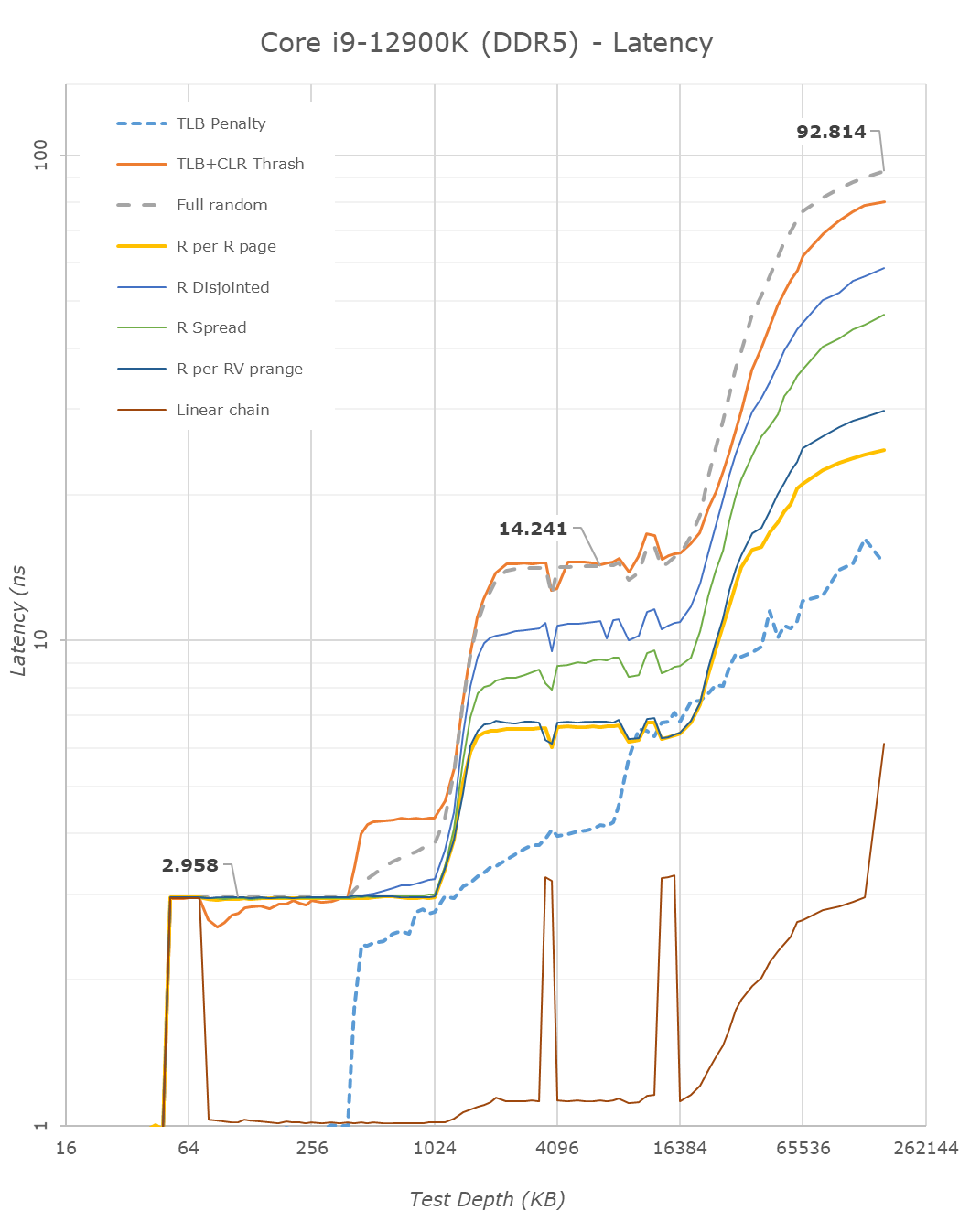
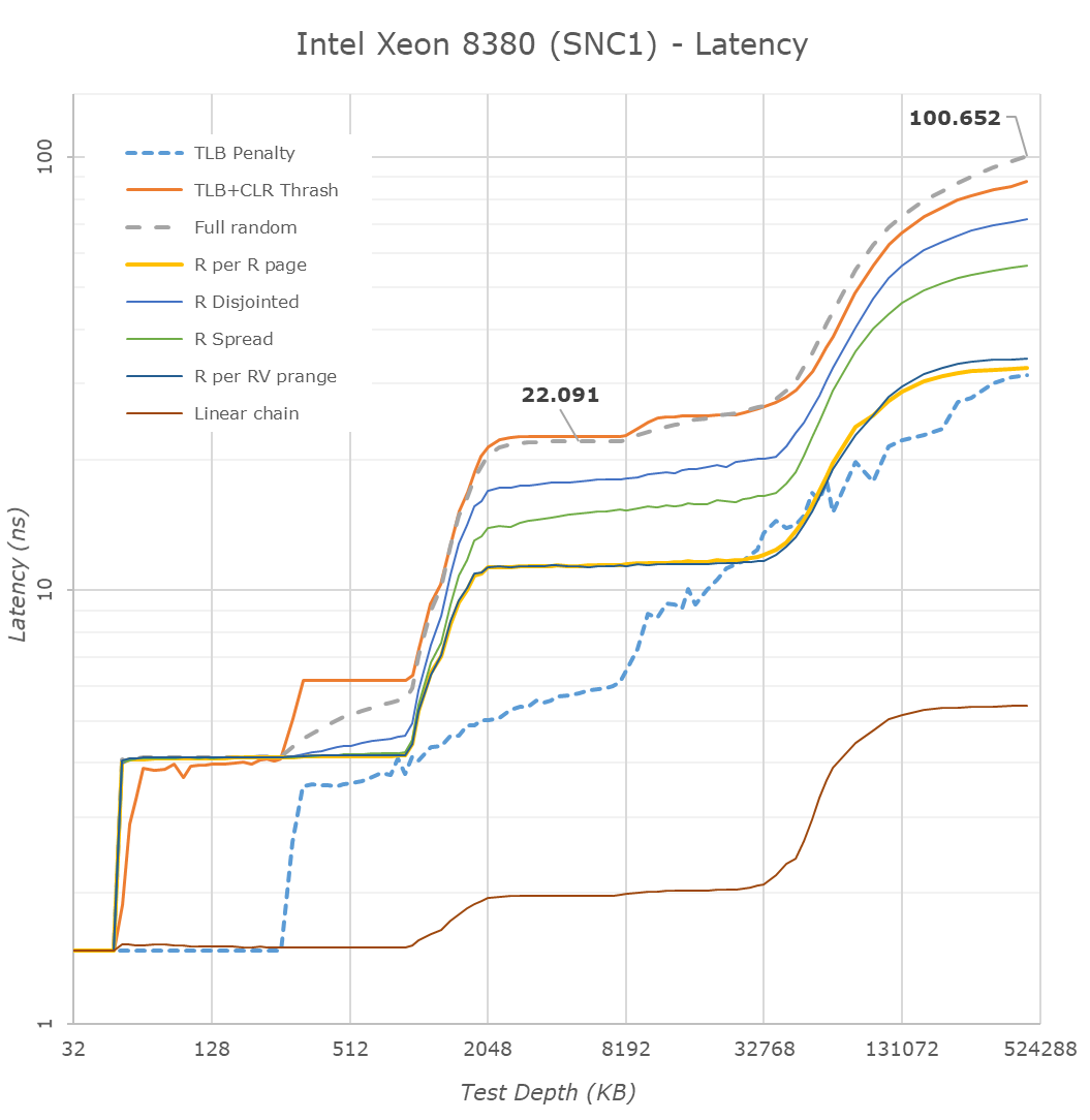
I think they kept it for latency reasons because gaming depends more on latency and the latency penalty from mesh isn't worth it.
If you simply count hops, a mesh is more efficient at even 12 stops. Try drawing a 4x3 grid on a piece of paper. Even if you put the memory controller in one corner (FWIW, I don't see why it couldn't be in the middle), the worst-case distance is only 5 hops. On a ring bus, it would be 6. So, maybe 12 was the point where it makes more sense to use a mesh than ring bus? I don't know how many stops Alder Lake has, but don't forget to include the iGPU, PCIe interface, and memory controller. That should bring it to at least 13, but then there's other stuff like the security processor... so maybe 14?

Raptor Lake's 24C/32T is 8 P-cores & 16 E-cores.
Those 16 E-cores eats the die area of 4 P-cores.
Sorry to burst your bubble, but 16 P-cores would clobber 24C/32T any day of the week.
First, 8 + 4 = 12. So, you wouldn't get 16 P-cores in the same die area (i.e. same price). Just so we're clear.

However, the reason I said 16 E-cores added more performance than 8 P-cores is based on the single-thread performance comparison that puts a single E-core at somewhere between 0.54 and 0.6 of a single thread on a P-core. If that extrapolated linearly, you'd get performance equivalent to between 8.64 and 9.6 P-cores. However, we know that performance doesn't scale linearly in either case.

The above stats I computed in post #32 indeed showed that the fully-loaded P-cores with 2 threads provided SPEC bench performance equivalent to a little more than 20 E-cores. That suggests you're right that 16 P-cores would beat a 8P + 16E configuration. But, you're forgetting about a key detail, which is power. In the 2Tx 8P scenario, Alder Lake is using 239 W. In the all E-core scenario, it's using only 48. So, without massively increasing your power budget, a 16 P-core CPU wouldn't get you nearly 20 E-cores worth of performance. And therefore, a 8P + 16E setup is going to vastly outperform a 12P setup.

This is not a controversial statement. Just look at the data.

And Intel does it because they're stingy and doesn't want to give consumers "Too many P-cores".
They're stingy in the way all corporations are stingy. However, they need to stay competitive. If the most cost-effective way to provide a competitive offering were with all P-cores, then they would do it. The fact that they didn't says they believe E-cores are a more cost-effective and power-efficient way to add compute, and the data we have backs them up on that.

The point is that giving Heterogenous Architecture onto DeskTop isn't nearly as necessary when Intel customers and many desktop customers don't care and are willing to OC or pump up the Wattage to get as much performance as the power delivery on their MoBo's allows. Many users on DeskTop, especially enthusiasts unleash the power limits and see how far they can push their systems.
You grossly overestimate the number of such overclockers. Intel caters to this community with special SKUs, but only because they know it's a vocal and high-profile subset of the user community.

They know that if they shipped 300 W desktop CPUs, it would be a market failure, because most reviewers test with non-exotic setups, not to mention that most users don't want extreme cooling solutions and would be disappointed with the products otherwise.

Anyway, they still have the upcoming Sapphire Rapids workstation CPUs as an opportunity to deliver more P-cores to the people who really want them and are willing to spend the money. So, we'll have to see if they release HEDT versions, or simply market the Xeon W 2400 or 3400 CPUs to the gaming community.
 
  • Like
Reactions: TJ Hooker

bit_user

Polypheme
Ambassador
Did they ONLY set affinities in the only E-core test or did they use affinities (instead of disabling cores in BIOS) for all the other tests?
Their explanation involving affinities just mentioned the E-cores. I don't know why they wouldn't just use BIOS for the other cases, as that's both easier and a better solution.

If they only did affinities then the ring/bus performance issue would could still be present in all the tests.
In the E-core only test, the ring-bus effects are unavoidable no matter what. So, the only question is whether they used affinities in the other cases, which I doubt.
 
Their explanation involving affinities just mentioned the E-cores. I don't know why they wouldn't just use BIOS for the other cases, as that's both easier and a better solution.


In the E-core only test, the ring-bus effects are unavoidable no matter what. So, the only question is whether they used affinities in the other cases, which I doubt.
They do say, "easier to set affinities to the various cores," which leads me to believe they could've just been using affinities for these tests.
Also, more slow down can occur with contention for L3 and memory when e-cores are active, not just from the ring/bus speeds.

Not sure if they'll reply on an old article but I posted a comment asking for clarification on this. We'll see what they say.
 

Kamen Rider Blade

Distinguished
Dec 2, 2013
1,280
810
20,060
Recent estimates I've seen on the additional area needed for HyperThreading in x86 CPUs are about 2-3% of die area. Scaling that to more threads would be a little cheaper, because you've already got the structures in place to manage > 1 thread per core. So, mostly what you need to scale up would be the register files and adding a couple bits to some book keeping structures.
You would need alot more of everything once you start scaling up to 8-way IMO.
L1 I/D $ for AMD/Intel would need to scale to 192 KiB L1 I/D $ respectively before you can sub-divide down again.
Same with every other register / counter / buffer / etc.

You just need alot more of everything before you can scale and sub-divide down.

One thing I haven't mentioned about n-way SMT is that Intel has gone down this path at least twice, before. Their first couple generations of Atom CPUs had 4-way SMT. They got rid of it, when they switched from in-order to out-of-order. The second instance was the last generation of Xeon Phi, which had 2-way cores that were both out-of-order and 4-way SMT. That probably tells us that Intel isn't afraid to go there, when they think it makes sense.
Or early implementations didn't create real world results like they hoped for and they dropped it.

Oh, and the last I heard, their iGPUs had 7-way SMT. That was pre-Xe. I don't know if they've said how many threads per EU Xe uses. And speaking of GPUs, I think AMD's GCN had 12-way SMT, but I could be mistaken.
I've never heard of SMT on GCN to that degree.

I didn't pick up on what you meant by "Dynamic SMT", at first. Now that I understand, I'll credit you for an interesting idea... but it has a fatal flaw.

The CPU core cannot decide, on its own, whether or not to simply ignore one of its threads. When the OS schedules a thread to run, it needs for that thread to get execution time. To violate that presumption will cause system-level performance degradation, if not worse. The reason is that the operating system has way more information about threads than a core can know. The OS will schedule threads to run when an I/O operation completes, or when an exclusive resource becomes available. There are sometimes other threads in line for that same resource, which means a CPU core arbitrarily starving out threads can cause a logjam effect.
Ok, then we can keep the Thread Information and stats available for the OS to use as needed.

Truly, the best approach to this problem is for something like the Thread Director to collect stats on threads, and then the OS can take those performance characteristics into account, when it decides which threads to schedule on which cores and when.
You mean provide more detailed info to the OS?


But video encoders don't scale well to lots of CPU threads and my point was that things which do tend to run well on GPUs.
It depends, but FFMPEG does scale well to a point, but after that your video quality will degrade.
But you could also run concurrent encodes of multiple files.

3D rendering however does scale well with more cores =D.


No, it wasn't competitive because the number of cells per die area wasn't competitive with 3D NAND.
That's not why I cared about it. I cared about Optane because of it's:
  • Utlra low latency, literally orders of magnitude lower
  • Ultra high reliability / Write Endurance. It had Write Endurance levels similar to HDD's. Something modern 3D NAND is getting worse with every time you increase the number of bits per cell.
  • Consistent performance regardless of how much of the storage was used or how degraded / fragmented the data was
  • Phenominal QD1 performance and Random Read/Write performance
The physics problem is the question of how small you can make them and in how many layers. I don't know the answer to that, but probably Intel does. Without knowing the answer, we cannot say whether the technology could ever be price-competitive with NAND.
Then we find it's niche and use it for that niche.


Hybrid CPUs, chiplets, and tiles don't sound like things risk-averse companies would generally do.
Chiplets & Tiles was writing on the wall, Intel needed to follow what AMD & the rest of the industry are already doing.
Hybrid isn't new either. ARM has been doing it for a VERY LONG time.

If Intel thinks enough people want only E-cores in a mainstream desktop socket, they'll make such a CPU. There's nothing else keeping them from doing it.
It's more of a PM (Product Manager) issue in how to design their desktop product stack.
Right now, I think they're just reusing the same designs and tuning them for DeskTop & Mobile while sharing the same fundamental dies.

The reason I think it won't happen is that most mainstream users are running some kind of interactive software that depends largely on single-thread performance for its responsiveness. Even if it's just a web browser. That's why the only two markets where you see them selling E-core only CPUs are at the extreme low end (i.e. chromebooks) and for servers that won't be running interactive workloads.
Software was already plenty responsive, especially well written ones that are native for Windows written in C/C++ and not programming abominations like MS Teams & and it's web based focused programming that's slow as eff.

Basically, the same thing applies to AMD and their Zen 4c strategy.
I can see end users wanting a similar result from AMD once Zen 4C launches and we get to see the cores.

You're free to have dedicated machines, if you're willing to pay the price. Modern software technology makes that largely unnecessary, unless you're a hardcore gamer who cannot tolerate the loss of even a couple fps.
I'm wiling to pay the price, I've been doing it for ages already.
I'm picky about how I want my OS to run along with my games.
I like dedicated boxes for certain programs with nothing in the background interfering.

In case you haven't noticed, there's been a long trend of virtualization being used to consolidate services onto fewer physical machines, because it's more efficient and cost-effective. Again, do what you want, but be aware that there are other options and an entire trend that you're going against.
I guess I go against that trend. I'm for more bare metal performance and seperating core apps onto dedicated machines for maximum performance.
I don't want to deal with Virtualization or suffer any performance penalties or oddities of Virtualization.
That's the way I roll, and I'm perfectly happy with it.


If you simply count hops, a mesh is more efficient at even 12 stops. Try drawing a 4x3 grid on a piece of paper. Even if you put the memory controller in one corner (FWIW, I don't see why it couldn't be in the middle), the worst-case distance is only 5 hops. On a ring bus, it would be 6. So, maybe 12 was the point where it makes more sense to use a mesh than ring bus? I don't know how many stops Alder Lake has, but don't forget to include the iGPU, PCIe interface, and memory controller. That should bring it to at least 13, but then there's other stuff like the security processor... so maybe 14?
Here's IRL test results from AnandTech:

KeiFheP.png
AlderLake's P-Core latency on the Ringbus is great since it offers between 23.# -> 35.# ns

OEfZ6jU.png
Notice how Core to Core Latency for Mesh within it's CPU domain is between 42-49 ns.

Here's Zen 3:
OQUs2Bf.png
Notice how Zen 3 with it's direct connect and potential hybrid interconnect that I theorized offers 14.#-19.# ns latency


First, 8 + 4 = 12. So, you wouldn't get 16 P-cores in the same die area (i.e. same price). Just so we're clear.
But you'd rather have 16 P-cores instead of 8x P-cores & 16x E-cores if given the choice to buy (Assuming you had the funds).

However, the reason I said 16 E-cores added more performance than 8 P-cores is based on the single-thread performance comparison that puts a single E-core at somewhere between 0.54 and 0.6 of a single thread on a P-core. If that extrapolated linearly, you'd get performance equivalent to between 8.64 and 9.6 P-cores. However, we know that performance doesn't scale linearly in either case.
Now you get why I want a literal dedicated SKU comprised of ALL E-cores.

The P-cores won't have any down-sides in terms of Ringbus slow down since they're all homogenous.

The above stats I computed in post #32 indeed showed that the fully-loaded P-cores with 2 threads provided SPEC bench performance equivalent to a little more than 20 E-cores. That suggests you're right that 16 P-cores would beat a 8P + 16E configuration. But, you're forgetting about a key detail, which is power. In the 2Tx 8P scenario, Alder Lake is using 239 W. In the all E-core scenario, it's using only 48. So, without massively increasing your power budget, a 16 P-core CPU wouldn't get you nearly 20 E-cores worth of performance. And therefore, a 8P + 16E setup is going to vastly outperform a 12P setup.
But you forget that Desktop users don't really care about power consumption and MoBo vendors have one button OCing, if not out-right OCing out of the box and providing above Intel rated Stock Power Levels to help with OCing.
Gamers Nexus literally made a video complaining how all MoBo manufacturers were basically ignoring Intel Stock Frequencies & Power Targets and OCing by default to one up each other in a arms race.

We're already in a race to consume more power to get maximum performance and go past the sweet spot in terms of efficiency.
Almost all the DeskTop users only want to see CPU go fast. Power Consumption & Heat Output be damned.
With all P-cores, no matter the core count, we will blow past the power budget to whatever the maximum VRM setup the MoBo can run to.
Same with E-cores, we'll blow past the power budget and OC the crap out of everything to push the VRM setups to the limit of wht the MoBo can run to.

This is not a controversial statement. Just look at the data.
Ko0b7gX.jpg
I want my personal server in a Desktop, I can imagine a Dual Tile "All E-core" setup with 80x E-cores.
That's going to be AMAZING.
And Sapphire Rapids with 56x Quad E-core Clusters = 224x E-cores.
That will be a beast in itself for so many reasons.

I want to shift the paradigm of having a "Home Server" in a standard ATX form factor box.

They're stingy in the way all corporations are stingy. However, they need to stay competitive. If the most cost-effective way to provide a competitive offering were with all P-cores, then they would do it. The fact that they didn't says they believe E-cores are a more cost-effective and power-efficient way to add compute, and the data we have backs them up on that.
I just think they are being cheap and don't want to manufacture different die's yet because they aren't on chiplets at this point in time.
They have to share the die designs between DeskTop & mobile.
So they don't want to make more Die Masks then necessary due to the incredible costs of a Die mask.


You grossly overestimate the number of such overclockers. Intel caters to this community with special SKUs, but only because they know it's a vocal and high-profile subset of the user community.
Damn Straight, we need to grow our numbers and become even more vocal.

They know that if they shipped 300 W desktop CPUs, it would be a market failure, because most reviewers test with non-exotic setups, not to mention that most users don't want extreme cooling solutions and would be disappointed with the products otherwise.
Yet AlderLake proves otherwise with the 12900K, it can easily go past 300 watts and end users don't care.

1XTC8I3.png

Anyway, they still have the upcoming Sapphire Rapids workstation CPUs as an opportunity to deliver more P-cores to the people who really want them and are willing to spend the money. So, we'll have to see if they release HEDT versions, or simply market the Xeon W 2400 or 3400 CPUs to the gaming community.
Sapphire Rapids was never meant for gamers, it's a Enterprise only product.
The only HEDT product coming is the rumored FishHawk Falls.
That's a rumored 24-core Monolithic Mesh interconnect setup.
 
Last edited:

bit_user

Polypheme
Ambassador
You would need alot more of everything once you start scaling up to 8-way IMO.
L1 I/D $ for AMD/Intel would need to scale to 192 KiB L1 I/D $ respectively before you can sub-divide down again.
Same with every other register / counter / buffer / etc.
The main thing you have to scale up with SMT is L1 & L2 cache. As for the rest, no... you shouldn't have to scale it by too much. One of SMT's benefits is latency-hiding, which means you don't need such a long OoO window and therefore shouldn't need to increase your shadow registers by much.


Or early implementations didn't create real world results like they hoped for and they dropped it.
CPU design is a multi-factorial optimization problem. Change one variable and you have to go back and optimize the others. CPU architects surely know this. Thus, they know that whatever someone experienced with SMT like 10 years ago isn't necessarily valid in modern microachitectures.

I've never heard of SMT on GCN to that degree.
I'm not 100% certain, but somewhat. If you have better information, post it.

Ok, then we can keep the Thread Information and stats available for the OS to use as needed.

You mean provide more detailed info to the OS?
Yes, that's what I'm saying.

That's not why I cared about it. I cared about Optane because of it's:
  • Utlra low latency, literally orders of magnitude lower
  • Ultra high reliability / Write Endurance. It had Write Endurance levels similar to HDD's. Something modern 3D NAND is getting worse with every time you increase the number of bits per cell.
  • Consistent performance regardless of how much of the storage was used or how degraded / fragmented the data was
  • Phenominal QD1 performance and Random Read/Write performance
Then we find it's niche and use it for that niche.
I understand all of that that. However, if Intel could not keep the price ($/GB) within a certain multiple of NAND, then it ends up being non-competitive for them.

Again, I'm not claiming to know that they had no viable path forward, but I'm suggesting one possible explanation for their actions that could not be addressed through different business & marketing practices. Whatever the actual truth is, we may never know (unless someone else does a version of the same tech as is able to make a go of it).

Hybrid isn't new either. ARM has been doing it for a VERY LONG time.
Hybrid on the desktop is pretty cutting edge, though. It has hit plenty of snags and has lots of detractors. I think it was a bold move, on their part.

It's more of a PM (Product Manager) issue in how to design their desktop product stack.
Right now, I think they're just reusing the same designs and tuning them for DeskTop & Mobile while sharing the same fundamental dies.
No, they have different dies for desktop vs. mobile. They made a conscious decision to put E-cores on the upper-end desktop CPUs, whether you like it or not. And it has generally worked out for them, in terms of winning benchmarks on highly-threaded workloads.

https://en.wikipedia.org/wiki/Alder_Lake#Dies

Software was already plenty responsive, especially well written ones that are native for Windows written in C/C++
Nah, games and plenty of application benchmarks are still largely dominated by single-threaded performance.

and not programming abominations like MS Teams & and it's web based focused programming that's slow as eff.
Like it or not, Intel and AMD have to build CPUs for the software people actually run, not what they wish people would run.

That said, Intel has done a lot to improve performance through its own open source libraries and through patches to GCC, LLVM, Linux kernel, and core open source libraries.

Here's IRL test results from AnandTech:
Three problems with that analysis:
  1. Xeon 8280 has 28 nodes, but you're comparing it to a CPU with 12. Try a mesh with 12 nodes and the results would look more comparable.
  2. You compared Alder Lake (Intel 7) to Cascade Lake (14 nm+++). Also, Skylake/Cascade Lake were the first generation of Intel CPUs to use a mesh, so it should be more refined in newer models.
  3. This is core-to-core latency, rather than core-to-memory latency. Core-to-core is a lot less common than core-to-memory communication. They're just showing you this data because it's interesting and revealing, not because it's actually relevant.
I would say let's look at Ice Lake SP, but that's a 40-core die, so even more disparate with the 12-node Alder Lake.

Oh, and previously you were lauding Intel's decision to pack the E-cores in quads that each share a single ring stop, but your own data shows they gain no benefit from being in quads and suffer a considerable penalty.

The plots you should be looking at are these. Here's Alder Lake i9-12900K (8+8 cores):

latency-ADL5.png


And here's Xeon Platinum 8380 (40 cores):

latency-8380-snc1.png


Now you get why I want a literal dedicated SKU comprised of ALL E-cores.
Eh, no. Not if you're in the same power envelope, in each case.

The P-cores won't have any down-sides in terms of Ringbus slow down since they're all homogenous.
Again, the stuff about the ring bus penalty of the E-cores isn't fundamental to E-cores, it's just a deficiency with their implementation in Alder Lake. We'll have to see if Raptor Lake fixed that. If not, then probably in Meteor Lake.

But you forget that Desktop users don't really care about power consumption
Sorry, we're just going to have to disagree on that. It's not just power consumption, but also the cost, size, weight, and noise of the cooling required for extreme power consumption. And even if the raw power consumption isn't that expensive, don't forget about air conditioning costs.

Plus, don't think Alder Lake's power requirements aren't contributing to the high cost of its motherboards. Complaints about their expense are commonplace.

Gamers Nexus literally made a video complaining how all MoBo manufacturers were basically ignoring Intel Stock Frequencies & Power Targets and OCing by default to one up each other in a arms race.
It's Intel's fault for letting them. The counterexample of AMD proves this.

Almost all the DeskTop users only want to see CPU go fast. Power Consumption & Heat Output be damned.
No, just the ones you see & hear on Youtube and elsewhere. Again, they represent a very vocal and visible minority of the market, but it is a minority.

Same with E-cores, we'll blow past the power budget and OC the crap out of everything to push the VRM setups to the limit of wht the MoBo can run to.
Did you not see where Anandtech's all E-core power consumption was only 48 W? Even a 32 E-core CPU shouldn't use as much power as just Alder Lake's 8 P-cores.

And Sapphire Rapids with 56x Quad E-core Clusters = 224x E-cores.
Sierra Forest is said to use a newer generation of E-core, which I'm guessing will have AVX-512 and therefore won't be quite so small. So, it could be more like 128 - 192 E-cores per CPU.

I want to shift the paradigm of having a "Home Server" in a standard ATX form factor box.
You can already find server boards for Intel's biggest CPUs in mini-ITX, if you really wanted. They don't have enough DIMM slots for all channels, but you already have your choice of form factor.

I just think they are being cheap and don't want to manufacture different die's yet because they aren't on chiplets at this point in time.
They have to share the die designs between DeskTop & mobile.
So they don't want to make more Die Masks then necessary due to the incredible costs of a Die mask.
I guess you've never heard of Snow Ridge? It's a specialty product for 5G base stations and such, with up to 24 E-cores. It proves they're willing to do it, if they think there's a market.

https://ark.intel.com/content/www/u...el-atom-processor-p5362-27m-cache-2-2ghz.html

Too bad I haven't seen them on any embedded server boards available to the general public.

Sapphire Rapids was never meant for gamers, it's a Enterprise only product.
They could still do something with their Xeon W version that's a nod towards gamers. They did that with Cascade Lake, by removing the usual restrictions preventing Xeons from being overclocked.
 
Last edited:
  • Like
Reactions: TJ Hooker

Kamen Rider Blade

Distinguished
Dec 2, 2013
1,280
810
20,060
The main thing you have to scale up with SMT is L1 & L2 cache. As for the rest, no... you shouldn't have to scale it by too much. One of SMT's benefits is latency-hiding, which means you don't need such a long OoO window and therefore shouldn't need to increase your shadow registers by much.
We'll see, I have a feeling that what I want to do with Dynamic SMT 1-8 would require far more shadow registers and increases on other things like OOO buffer size by alot more given the scale I want things to work. But that's a different issue.


CPU design is a multi-factorial optimization problem. Change one variable and you have to go back and optimize the others. CPU architects surely know this. Thus, they know that whatever someone experienced with SMT like 10 years ago isn't necessarily valid in modern microachitectures.
True

I'm not 100% certain, but somewhat. If you have better information, post it.
Ok

Yes, that's what I'm saying.
Fair enough

I understand all of that that. However, if Intel could not keep the price ($/GB) within a certain multiple of NAND, then it ends up being non-competitive for them.
But that issue has to do with scaling to multiple memory manufacturers and getting them all in on it.
At the time, they only had Micron as a sole source provider. They didn't involve all the other Memory manufacturers for whatever reason.
Licensing, fees, Micron doesn't want to share the IP/Tech or license it out for whatever reason, etc.

Again, I'm not claiming to know that they had no viable path forward, but I'm suggesting one possible explanation for their actions that could not be addressed through different business & marketing practices. Whatever the actual truth is, we may never know (unless someone else does a version of the same tech as is able to make a go of it).
Hopefully somebody comes up with similar tech or makes this one work in the future.

Hybrid on the desktop is pretty cutting edge, though. It has hit plenty of snags and has lots of detractors. I think it was a bold move, on their part.
Ok, I guess we'll have to agree to disagree since I don't see it as that bold of a move.

No, they have different dies for desktop vs. mobile. They made a conscious decision to put E-cores on the upper-end desktop CPUs, whether you like it or not. And it has generally worked out for them, in terms of winning benchmarks on highly-threaded workloads.

https://en.wikipedia.org/wiki/Alder_Lake#Dies
I know they won benchmarks because of them, that's not what I'm contesting.
I just think they would end up with better overall results going my suggested route.
But we'll agree to disagree on what route to take.


Nah, games and plenty of application benchmarks are still largely dominated by single-threaded performance.
Most modern games are pretty multi-threaded across the board.
Most of the professional apps, minus a few major outliers, are pretty much multi-threaded.

Like it or not, Intel and AMD have to build CPUs for the software people actually run, not what they wish people would run.
Or we need companies to fix their software development teams to not suck.
MS & Adobe, I'm looking at you.

That said, Intel has done a lot to improve performance through its own open source libraries and through patches to GCC, LLVM, Linux kernel, and core open source libraries.
I'm always a bit skeptical with Intel and their "Software Contributions". After being found guilty of Anti-Trust, they also pulled shenanigans with their math libraries to screw over non Intel CPU's that Agner Fog has detailed.
So I always want extra eyes on anything Intel contributes to make sure they don't do shady crap again.


Three problems with that analysis:
  1. Xeon 8280 has 28 nodes, but you're comparing it to a CPU with 12. Try a mesh with 12 nodes and the results would look more comparable.
  2. You compared Alder Lake (Intel 7) to Cascade Lake (14 nm+++). Also, Skylake/Cascade Lake were the first generation of Intel CPUs to use a mesh, so it should be more refined in newer models.
  3. This is core-to-core latency, rather than core-to-memory latency. Core-to-core is a lot less common than core-to-memory communication. They're just showing you this data because it's interesting and revealing, not because it's actually relevant.
I would say let's look at Ice Lake SP, but that's a 40-core die, so even more disparate with the 12-node Alder Lake.
Core to Core Latency is important for Multi-threading and cross thread communication.
As for Latency to Memory Access and what level of memory, that's a completely different subject matter.

Oh, and previously you were lauding Intel's decision to pack the E-cores in quads that each share a single ring stop, but your own data shows they gain no benefit from being in quads and suffer a considerable penalty.
That's more to do with how Intel architectured their communication pipeline between cores then the fundamentals of using a Quad setup.

The plots you should be looking at are these. Here's Alder Lake i9-12900K (8+8 cores):

latency-ADL5.png


And here's Xeon Platinum 8380 (40 cores):

latency-8380-snc1.png
Yes, I understand memory access latency, but that's a seperate issue that mostly involves the memory controller and how fast L1/L2/L3 access is.
But that's a different topic than the one I was trying to talk about.

Eh, no. Not if you're in the same power envelope, in each case.
You can tune the settings to have a lower base and higher boost, but that's about how you want to tune it.
I don't mind higher power usage in general, so does many folks.

Again, the stuff about the ring bus penalty of the E-cores isn't fundamental to E-cores, it's just a deficiency with their implementation in Alder Lake. We'll have to see if Raptor Lake fixed that. If not, then probably in Meteor Lake.
Yes, we'll see, in due time.

Sorry, we're just going to have to disagree on that. It's not just power consumption, but also the cost, size, weight, and noise of the cooling required for extreme power consumption. And even if the raw power consumption isn't that expensive, don't forget about air conditioning costs.
The cost of the cooling solution isn't that big of a deal, we have plenty of cost effective solutions in this day and age.
And as far as AC costs, that just depends on where you live.

Plus, don't think Alder Lake's power requirements aren't contributing to the high cost of its motherboards. Complaints about their expense are commonplace.
But alot of that costs has to do with excessive precision and parts needed for next gen PCIe standards along with many other pointless embelishments to MoBo design.
We've always had varying size of VRM power levels based on what tier of MoBo you want to purchase.
Modern MoBo designs more resemble fine artwork than functional designs first and artistry 2nd/3rd/4th like the good ole days.

It's Intel's fault for letting them. The counterexample of AMD proves this.
I think Intel doesn't mind, that's why they let them do that.
Intel just wants to win Benchmarks at all costs, so they don't care about wasting power.

No, just the ones you see & hear on Youtube and elsewhere. Again, they represent a very vocal and visible minority of the market, but it is a minority.
We'll have to agree to disagree. If you're in the market for a Top of the line CPU SKU, then you know what you're getting yourself into.
Power Consumption & Heat Generation along with operating costs that goes with it.

Did you not see where Anandtech's all E-core power consumption was only 48 W? Even a 32 E-core CPU shouldn't use as much power as just Alder Lake's 8 P-cores.
That's a "P-core" design issue, and usage of AVX3-512 makes power consumption that much worse as well along with having a frequency penalty.
That's why I don't see E-cores getting AVX3-512 anytime soon since it would balloon the power consumption of E-cores unnecessarily and add too much transistor budget requirement in the FPU that the size of the Quad E-core cluster would balloon. E-cores might never even get AVX3-512 because the power requirements to run such code is insane compared to AVX2-256.


Sierra Forest is said to use a newer generation of E-core, which I'm guessing will have AVX-512 and therefore won't be quite so small. So, it could be more like 128 - 192 E-cores per CPU.
I personally doubt they'll add in AVX3-512 to "E-cores" based on my above reasoning.
But we'll see soon enough.

You can already find server boards for Intel's biggest CPUs in mini-ITX, if you really wanted. They don't have enough DIMM slots for all channels, but you already have your choice of form factor.
It's more about having more options for standard ATX MoBo's for me.
I really don't care for mini-ITX.


I guess you've never heard of Snow Ridge? It's a specialty product for 5G base stations and such, with up to 24 E-cores. It proves they're willing to do it, if they think there's a market.

https://ark.intel.com/content/www/u...el-atom-processor-p5362-27m-cache-2-2ghz.html

Too bad I haven't seen them on any embedded server boards available to the general public.
That doesn't sound like a part I can pickup at Micro-center.


They could still do something with their Xeon W version that's a nod towards gamers. They did that with Cascade Lake, by removing the usual restrictions preventing Xeons from being overclocked.
I think FishHawk Falls will be that nod. I'm looking forward to see what they do with it.
 

bit_user

Polypheme
Ambassador
But that issue has to do with scaling to multiple memory manufacturers and getting them all in on it.
Do you understand that Optane uses a different fundamental technology?

How can you say it would continue to be viable when you don't even know how it works? We know it's roughly similar to memristor-class devices, but without knowing the details, nobody can really say whether the storage cells could continue to be shrunk without compromising their key properties.

At the time, they only had Micron as a sole source provider. They didn't involve all the other Memory manufacturers for whatever reason.
Licensing, fees, Micron doesn't want to share the IP/Tech or license it out for whatever reason, etc.
Intel created it as a technology partnership with Micron. However, when they split up, they sabotaged Micron's ability to continue developing it. Intel sued Micron, for trying to keep some of the critical people and IP.

However, Intel still had a way to produce it without Micron. They did have an entire nonvolatile memory business (including fabs), in case you didn't know.


I don't remember the details, but I think that fab was not included in their sale nonvolatile memory assets to SK Hynix (i.e. producing the company known as Solidigm).

Hopefully somebody comes up with similar tech or makes this one work in the future.
There's a company called Crossbar Inc. that's been developing memristor-based storage since 2010.


Most modern games are pretty multi-threaded across the board.
Most of the professional apps, minus a few major outliers, are pretty much multi-threaded.
The balance of work is not symmetrical. The way a lot of games are multi-threaded, you have a couple of threads orchestrating everything, and you want them to run fastest.

But, there's another reason why lightly-threaded performance matters, and that's for the tail of any workload. When you look at a profile of the work involved in a multithreaded task, there are often portions where only a few threads are active, especially at the end. If the CPU has faster threads it can use for these portions, then it has a marked effect on reducing the overall time.

Let's look at this another way. Given that Intel's E-cores are superior in perf/W and perf/area (which also means perf/$), why would they even bother with P-cores if they didn't really make a difference? They could've just smashed AMD with a 40-core chip consisting of all E-cores, if that were all it took.

Core to Core Latency is important for Multi-threading and cross thread communication.
I didn't say it's not, but it's not nearly as important as memory latency. The quantity of core-to-memory transactions is hundreds or thousands of times greater than core-to-core.

Yes, I understand memory access latency, but that's a seperate issue that mostly involves the memory controller and how fast L1/L2/L3 access is.
Memory & L3 access latency are both very dependent on the design of the interconnect network.

The cost of the cooling solution isn't that big of a deal, we have plenty of cost effective solutions in this day and age.
And as far as AC costs, that just depends on where you live.
My own experience is this: I mostly work in an upstairs room since Covid hit. During the warm months, I limit myself to a 45 W laptop that I tuned to run closer to 25 W. I also have a workstation with a 140 W CPU and a 275 W dGPU that I avoid turning on, until I can open windows in the evening, because my summer power bill is already in the neighborhood of $100/month and if I turn on the A/C to cool that upstairs room, I have to turn it on for my entire home.

I don't know how many people are in a similar boat, but I'd bet more than a few. I will not be replacing this workstation with anything as power-hungry.

Yes, if I really needed to run my workstation all day, I could perhaps get a window A/C unit for that room, but it's not worth it to me. The room has one window that I prefer to look out of, when I'm sitting at my desk.

That's a "P-core" design issue, and usage of AVX3-512 makes power consumption that much worse as well along with having a frequency penalty.
Those core/power scaling measurements were not using AVX-512.

That's why I don't see E-cores getting AVX3-512 anytime soon since it would balloon the power consumption of E-cores unnecessarily and add too much transistor budget requirement in the FPU that the size of the Quad E-core cluster would balloon.
Competitive pressure will force their hand, even if they didn't intend to do it otherwise. Lunar Lake and (I think) Sierra Forest are due to be produced on the "Intel 4" node, and will use a new E-core design. I'll bet those E-cores will have AVX-512.

It's more about having more options for standard ATX MoBo's for me.
I really don't care for mini-ITX.
Right, but but the point was you already have your choice of form factor for just about any CPU.

That doesn't sound like a part I can pickup at Micro-center.
The point was that Intel is already quite willing to make chips with lots of E-cores, if they think there's a market.
 

Kamen Rider Blade

Distinguished
Dec 2, 2013
1,280
810
20,060
Do you understand that Optane uses a different fundamental technology?
Yes, it's based on Phase Change memory.

How can you say it would continue to be viable when you don't even know how it works? We know it's roughly similar to memristor-class devices, but without knowing the details, nobody can really say whether the storage cells could continue to be shrunk without compromising their key properties.
I know that there were plans on scaling it down according to their product managers and I really only have their words to trust.


Intel created it as a technology partnership with Micron. However, when they split up, they sabotaged Micron's ability to continue developing it. Intel sued Micron, for trying to keep some of the critical people and IP.
Yeah, it's quite the cluster f### of a situation.

However, Intel still had a way to produce it without Micron. They did have an entire nonvolatile memory business (including fabs), in case you didn't know.
Didn't Intel sell of their memory business?


I don't remember the details, but I think that fab was not included in their sale nonvolatile memory assets to SK Hynix (i.e. producing the company known as Solidigm).
Yet I don't see them using that fab to crank out more Optane memory.

There's a company called Crossbar Inc. that's been developing memristor-based storage since 2010.

I hope they get their act together and make a competitive product.

The balance of work is not symmetrical. The way a lot of games are multi-threaded, you have a couple of threads orchestrating everything, and you want them to run fastest.

But, there's another reason why lightly-threaded performance matters, and that's for the tail of any workload. When you look at a profile of the work involved in a multithreaded task, there are often portions where only a few threads are active, especially at the end. If the CPU has faster threads it can use for these portions, then it has a marked effect on reducing the overall time.
Depends on the game and how it's architectured. But I've seen different loads then what you've seen.
But that's the beauty of game development, it all comes down to how they decided to architecture their game.

Let's look at this another way. Given that Intel's E-cores are superior in perf/W and perf/area (which also means perf/$), why would they even bother with P-cores if they didn't really make a difference? They could've just smashed AMD with a 40-core chip consisting of all E-cores, if that were all it took.
Because the E-core's Single Threaded Performance was barely past Skylake. Ergo it wasn't competitive on Single Threaded and only did well on MT when working with a massive # of it's sibling E-cores.


I didn't say it's not, but it's not nearly as important as memory latency. The quantity of core-to-memory transactions is hundreds or thousands of times greater than core-to-core.
Ok

Memory & L3 access latency are both very dependent on the design of the interconnect network.
Then I'm glad AMD is using a Serial based connection that is well architected and logical in layout.


My own experience is this: I mostly work in an upstairs room since Covid hit. During the warm months, I limit myself to a 45 W laptop that I tuned to run closer to 25 W. I also have a workstation with a 140 W CPU and a 275 W dGPU that I avoid turning on, until I can open windows in the evening, because my summer power bill is already in the neighborhood of $100/month and if I turn on the A/C to cool that upstairs room, I have to turn it on for my entire home.
I would highly recommend Ducted Mini-Split A/C's instead of whole house A/C's.

Yeah, it's kind of expensive to outfit your entire house with Ducted Mini-Split's. But it offers redundancy and you can turn on only the units you need, in the rooms you need.

And most of us in Asia/Europe have been using Ducted Mini-Split A/C's for generations.

Only in the US is Whole house A/C's really common.

I don't know how many people are in a similar boat, but I'd bet more than a few. I will not be replacing this workstation with anything as power-hungry.
Ok, that's your situation.

Yes, if I really needed to run my workstation all day, I could perhaps get a window A/C unit for that room, but it's not worth it to me. The room has one window that I prefer to look out of, when I'm sitting at my desk.
Portable A/C units are very efficient if you have a modern unit.

Those core/power scaling measurements were not using AVX-512.
I know, but I've seen the current core/power scaling w/o AVX3-512, & it's already that bad. Turning on AVX3-512 will only make it worse.

Competitive pressure will force their hand, even if they didn't intend to do it otherwise. Lunar Lake and (I think) Sierra Forest are due to be produced on the "Intel 4" node, and will use a new E-core design. I'll bet those E-cores will have AVX-512.
Ok, I'll bet that they won't due to wanting to keep the cores tiny.

AVX3-512 is very niche and I don't think average consumers will ever really benefit from it.

I agree with Linus Torvalds "I Hope AVX512 Dies A Painful Death".

AVX3-512 is a giant waste of transistors for the average consumer and it should be left to Enterprise / WorkStations as a specialized feature.

AVX2-256 is good enough for the vast majority of consumers, let's not fragment the consumer code base anymore.

Right, but but the point was you already have your choice of form factor for just about any CPU.
Some of the high end CPU's like ThreadRipper were only recently addressed for DIY consumers like myself.
I wish we would get more HEDT like parts similar to ThreadRipper.
I could wish for a new CPU platform called "FX" that has 6x CCD's maximum and they would sell it as a replacement for the old ThreadRipper / HEDT line.
3-6x CCD's would cover that market gap that currently exists between high end TR & regular consumer lines without intruding too much on TR.

The point was that Intel is already quite willing to make chips with lots of E-cores, if they think there's a market.
I just hope they include the average consumer and not just focus on Enterprise only.
 

bit_user

Polypheme
Ambassador
Ok, I'll bet that they won't due to wanting to keep the cores tiny.

AVX3-512 is very niche and I don't think average consumers will ever really benefit from it.
Well, they put AVX-512 in the Gen 10 laptop CPUs (Ice Lake) and Gen 11 laptop + desktop CPUs (Tiger Lake + Rocket Lake). So, I'm taking that as a sign that Intel disagrees on whether consumers benefit. More importantly, Sierra Forest is going to be a big reason for them to add it to their E-cores, because I'll bet that folks with server workloads won't want to recompile their code just to migrate from P-core Xeons to E-core Xeons. Or AMD 's Genoa or Begamo CPUs, for that matter.

The size impact can be mitigated like what AMD has done in Zen 4 - split the ALU in half. Your registers still have to be 512-bit, but between that and varying how many FMAs/core, I think it shouldn't totally blow up their E-cores on newer process nodes.

I read that and am of mixed opinions about it. On the one hand, you have to understand Linus' bias. He sees the cost of supporting AVX-512, in terms of things like context-switching overhead and other details the kernel has to worry about. And his performance focus is on kernel-centric workloads that involve lots of I/O, networking, thread scheduling, memory management, etc. - server stuff, mainly. So, he sees AVX-512 as baggage that's not really helping the things he worries about.

And another argument against AVX-512 is that it's moving CPUs further into the territory of computation that's best handled on GPUs and AI accelerators. And if you look at Intel's 14 nm CPUs which implement it, they generally have serious issues with clock-throttling. So, you can clearly make the case that Intel moved to 512-bit before the silicon technology was really ready for it.

Further, if you compare it to ARM's SVE, it's disappointing that Intel blew an opportunity to decouple the instruction coding from the implementation width.

So, there's no shortage of reasons to hate on it.

Proponents cite that it cleans up some things about AVX/AVX2 and can be used in 128-bit or 256-bit mode, if you don't need to use full 512-bit computation. Some say it's good for doing "just a little" vector computation that's interspersed with serial compute, where the overhead of shipping the work to a GPU wouldn't be worth it. There are also people who point out that CPUs are "good enough" at light AI workloads, that it's nice not to have to depend on having a GPU available. And still other people who see it as "moar, better ISA", and want to keep moving "forward". And finally, because Intel did it, there are those server users who simply want AMD to catch up, so they can run the same code everywhere.

On balance, I think it has more negatives than positives, but it was only a matter of time before the proponents convinced AMD. I'm glad AMD held out as long as they did, though. Anyway, those same forces are going to push Intel to have it in Sierra Forest.

Not to mention those few desktop programs that benefit from it, that Intel is going to want to win back from the AMD crowd. Since they've opted for the (IMO, smart but embarrassing & painful) route of symmetrical ISA on their hybrid CPUs, that means they're going to have to put AVX-512 in the E-cores, in order to re-enable it on the P-cores.

So, my prediction is that AVX-512 will return to Intel desktop CPUs for Meteor Lake. P-cores and E-cores.

I just hope they include the average consumer and not just focus on Enterprise only.
Your best and pretty much only chance is a Xeon W version of Sierra Forest.
 

Kamen Rider Blade

Distinguished
Dec 2, 2013
1,280
810
20,060
Well, they put AVX-512 in the Gen 10 laptop CPUs (Ice Lake) and Gen 11 laptop + desktop CPUs (Tiger Lake + Rocket Lake). So, I'm taking that as a sign that Intel disagrees on whether consumers benefit. More importantly, Sierra Forest is going to be a big reason for them to add it to their E-cores, because I'll bet that folks with server workloads won't want to recompile their code just to migrate from P-core Xeons to E-core Xeons. Or AMD 's Genoa or Begamo CPUs, for that matter.
Yet on Gen 12, Intel decided to fuse off AVX3-512. They could've just left it there and let end users access it by turning off E-cores.
But they went out of their way to fuse it off for some reason.

The size impact can be mitigated like what AMD has done in Zen 4 - split the ALU in half. Your registers still have to be 512-bit, but between that and varying how many FMAs/core, I think it shouldn't totally blow up their E-cores on newer process nodes.
From what I read or heard about Zen 4, they just use 2x 256 bit FPU registers from AVX2 to solve AVX3-512.
It isn't perfect, but it doesn't add that much transistor count to get AVX3-512 to work.
You don't seem to get the best performance boost, but it also doesn't seem to have much of a frequency penalty either.


I read that and am of mixed opinions about it. On the one hand, you have to understand Linus' bias. He sees the cost of supporting AVX-512, in terms of things like context-switching overhead and other details the kernel has to worry about. And his performance focus is on kernel-centric workloads that involve lots of I/O, networking, thread scheduling, memory management, etc. - server stuff, mainly. So, he sees AVX-512 as baggage that's not really helping the things he worries about.

And another argument against AVX-512 is that it's moving CPUs further into the territory of computation that's best handled on GPUs and AI accelerators. And if you look at Intel's 14 nm CPUs which implement it, they generally have serious issues with clock-throttling. So, you can clearly make the case that Intel moved to 512-bit before the silicon technology was really ready for it.
Why can't we just use GPU's to run the same code that was designed for AVX3-512?
Wouldn't have it been better off run on CUDA / GPU / OpenCL?

Further, if you compare it to ARM's SVE, it's disappointing that Intel blew an opportunity to decouple the instruction coding from the implementation width.

So, there's no shortage of reasons to hate on it.
From what I can tell, AVX3-512 was originally created as a new instruction set to dunk on AMD while solving the AI issue at the same time.
Now that AMD has made their implementation, Intel fuses it off in 12th Gen AlderLake killing consumer support and leaving it as a "Unique Xeon ONLY Feature".

Proponents cite that it cleans up some things about AVX/AVX2 and can be used in 128-bit or 256-bit mode, if you don't need to use full 512-bit computation. Some say it's good for doing "just a little" vector computation that's interspersed with serial compute, where the overhead of shipping the work to a GPU wouldn't be worth it. There are also people who point out that CPUs are "good enough" at light AI workloads, that it's nice not to have to depend on having a GPU available. And still other people who see it as "moar, better ISA", and want to keep moving "forward". And finally, because Intel did it, there are those server users who simply want AMD to catch up, so they can run the same code everywhere.
I'm just glad that AMD isn't spending much transistor budget on getting AVX3-512 to work.
Yeah, it might not be the most optimal / fastest implmentation, but AVX3-512 support isn't that important at this point in time due to lack of support.

Chicken & Egg problem.

On balance, I think it has more negatives than positives, but it was only a matter of time before the proponents convinced AMD. I'm glad AMD held out as long as they did, though. Anyway, those same forces are going to push Intel to have it in Sierra Forest.

Not to mention those few desktop programs that benefit from it, that Intel is going to want to win back from the AMD crowd. Since they've opted for the (IMO, smart but embarrassing & painful) route of symmetrical ISA on their hybrid CPUs, that means they're going to have to put AVX-512 in the E-cores, in order to re-enable it on the P-cores.

So, my prediction is that AVX-512 will return to Intel desktop CPUs for Meteor Lake. P-cores and E-cores.
But what implementation will they do if they do it.
I'm still doubtful that they'll do it, but time will tell.

Will the E-cores copy AMD and just double pump 2x 256-bit FPU registers to solve AVX3-512?
It won't be the fastest implementation, but it'll work.


Your best and pretty much only chance is a Xeon W version of Sierra Forest.
=(
Xeon's are out of my price range as a normal consumer.

I want consumer budget friendly DeskTop chips.
 

bit_user

Polypheme
Ambassador
Yet on Gen 12, Intel decided to fuse off AVX3-512. They could've just left it there and let end users access it by turning off E-cores.
But they went out of their way to fuse it off for some reason.
What you describe would've been a support nightmare.

Also, we don't know if there were errata in the hardware implementation, because Intel said they didn't validate AVX-512 in those products.

From what I read or heard about Zen 4, they just use 2x 256 bit FPU registers from AVX2 to solve AVX3-512.
No, that can't work. AVX-512 doubles the number of vector registers to 32, and then doubles their size. So, you need 4x as much register capacity as what AVX2 requires. Technically, they might implement everything with 256-bit registers, but that just means they need 64x 256-bit registers per thread, instead of the 16x 256-bit registers required by AVX2. There's no getting around it.

Perhaps what you're thinking of is their approach of breaking AVX-512 into two pieces and processing the halves serially. What's interesting is that I read someone claiming this was possible for AVX/AVX2, but not AVX-512. Perhaps that was based on certain instructions, such as a global permute, which I guess AMD could've handled as special cases.

Why can't we just use GPU's to run the same code that was designed for AVX3-512?
Wouldn't have it been better off run on CUDA / GPU / OpenCL?
If the code is written using something like OpenCL or OneAPI, then it can be targeted at either a CPU or GPU device. However, if it's written directly as AVX-512 code, then it basically needs to be rewritten to have the option of re-targeting it at a GPU.

In theory, you might have some kind of runtime translation, but it probably wouldn't work very well. To get good performance out of a GPU, you really need to think about data movement and locality, whereas a selling-point of AVX-512 is that you can just process the data in-situ of your normal application code.

Plus, there are probably a decent number of AVX-512 instructions that aren't actually SIMD. So, translating such code to run well on a GPU could be non-trivial.

From what I can tell, AVX3-512 was originally created as a new instruction set to dunk on AMD while solving the AI issue at the same time.
The AI-oriented subsets of AVX-512 came later. They aren't included in the "Foundation" part.

https://en.wikipedia.org/wiki/AVX-512#CPUs_with_AVX-512

But what implementation will they do if they do it.
I'm still doubtful that they'll do it, but time will tell.

Will the E-cores copy AMD and just double pump 2x 256-bit FPU registers to solve AVX3-512?
It won't be the fastest implementation, but it'll work.
The top 2 priorities of the E-cores are: area-efficiency and power-efficiency (and probably in that order). So, that will likely dictate their implementation.

=(
Xeon's are out of my price range as a normal consumer.
Xeon W starts < $1000 and goes up to about $4500 (that's a ceiling I think was basically set by Threadripper).

Obviously, the top end is a bit much, but if you're looking at high-end gaming PCs, then the first few tiers of Xeon W should be attainable.

I want consumer budget friendly DeskTop chips.
Don't we all?

What these companies build has a lot to do with the perceived demand. If you want to gin up demand for such a product, then perhaps your best bet is to pester a bunch of influencers and tech publications to explore the potential of different E-core -only CPU configurations.
 

Kamen Rider Blade

Distinguished
Dec 2, 2013
1,280
810
20,060
What you describe would've been a support nightmare.

Also, we don't know if there were errata in the hardware implementation, because Intel said they didn't validate AVX-512 in those products.
How convenient that they included AVX-512 support in the transistor layout, but decided to "not validate" it.
Seems like a wierd over sight. Why waste the transistor budget on AVX-512, then not validate that it works?


No, that can't work. AVX-512 doubles the number of vector registers to 32, and then doubles their size. So, you need 4x as much register capacity as what AVX2 requires. Technically, they might implement everything with 256-bit registers, but that just means they need 64x 256-bit registers per thread, instead of the 16x 256-bit registers required by AVX2. There's no getting around it.

Perhaps what you're thinking of is their approach of breaking AVX-512 into two pieces and processing the halves serially. What's interesting is that I read someone claiming this was possible for AVX/AVX2, but not AVX-512. Perhaps that was based on certain instructions, such as a global permute, which I guess AMD could've handled as special cases.
Never-mind about what I said. I watched the release video and various YT videos on Ryzen 7000. They're using a DDR style Double Pumping with AVX2-256 to solve AVX3-512.
So that's how they plan on implementing AVX3-512 with minimal transistor budget increase.
Smart IMO for the goals they planned on achieving.

If the code is written using something like OpenCL or OneAPI, then it can be targeted at either a CPU or GPU device. However, if it's written directly as AVX-512 code, then it basically needs to be rewritten to have the option of re-targeting it at a GPU.

In theory, you might have some kind of runtime translation, but it probably wouldn't work very well. To get good performance out of a GPU, you really need to think about data movement and locality, whereas a selling-point of AVX-512 is that you can just process the data in-situ of your normal application code.

Plus, there are probably a decent number of AVX-512 instructions that aren't actually SIMD. So, translating such code to run well on a GPU could be non-trivial.
But at that point, why not design your code for GPU's if you can? Why waste time for CPU's if you know it would run faster on GPU?
Unless the code is absolutely necessary for CPU operations, and there are some, then go with GPU if you can parallelize it.


The AI-oriented subsets of AVX-512 came later. They aren't included in the "Foundation" part.

https://en.wikipedia.org/wiki/AVX-512#CPUs_with_AVX-512
IC

The top 2 priorities of the E-cores are: area-efficiency and power-efficiency (and probably in that order). So, that will likely dictate their implementation.
Yup, that's why I don't think E-cores will increase in size.

Xeon W starts < $1000 and goes up to about $4500 (that's a ceiling I think was basically set by Threadripper).

Obviously, the top end is a bit much, but if you're looking at high-end gaming PCs, then the first few tiers of Xeon W should be attainable.
We'll see how it compares to Ryzen 7000 and the 7950X.

Don't we all?

What these companies build has a lot to do with the perceived demand. If you want to gin up demand for such a product, then perhaps your best bet is to pester a bunch of influencers and tech publications to explore the potential of different E-core -only CPU configurations.
=D
 

bit_user

Polypheme
Ambassador
How convenient that they included AVX-512 support in the transistor layout, but decided to "not validate" it.
Seems like a wierd over sight. Why waste the transistor budget on AVX-512, then not validate that it works?
The cores are the same for both desktop & server. I guess they were looking to save some money and maybe use the desktop chips as a test vehicle to find & fix some bugs in time for the Sapphire Rapids server CPUs?

Or... they really did plan on enabling AVX-512, but got cold feet after it was too late to remove it from the chip design. The CPU development pipeline is like 4 years, so maybe they got cold feet about enabling it at like year 3, when the design was mostly done but not validation?

Or... there's at least one Alder Lake die that actually has no E-cores. Perhaps it was their intention to enable AVX-512 on these, but decided not to for "marketing" reasons?

All we can do is speculate.

But at that point, why not design your code for GPU's if you can? Why waste time for CPU's if you know it would run faster on GPU?
Unless the code is absolutely necessary for CPU operations, and there are some, then go with GPU if you can parallelize it.
I happen to agree, but maybe Intel and AMD think there are enough customers who won't do this.
 

Kamen Rider Blade

Distinguished
Dec 2, 2013
1,280
810
20,060
All we can do is speculate.

Indeed, that was a VERY weird move by Intel.
Yeah, we know AVX3-512 doesn't run on E-cores currently, but to literally "FUSE OFF" AVX3-512 and tell the public that you didn't validate it?
Then you put down the transistors necessary to run it in your AlderLake CPU design?

That reeks of last minute changes. Like one thing happened by adding E-cores & Thread Director, and they weren't sure what to do about AVX3-512.

Then they changed their mind at last minute and tried to justify it publically.

I happen to agree, but maybe Intel and AMD think there are enough customers who won't do this.
I think it's more of Intel driving the force behind AVX3-512.
AMD has been in a "Wait & See" mode for adoption of AVX3-512 before they decide to add it in.
That's why it took AMD this long to release a CPU with it.

AMD wasn't in a rush to play the "Chicken & Egg" routine.

While Intel was using AVX3-512 as a "Gotcha" for performance on Benchmarks to try to convince people to buy Rocket Lake & Comet Lake.
 
  • Like
Reactions: bit_user