News AMD Shares New Second-Gen 3D V-Cache Chiplet Details, up to 2.5 TB/s

bit_user

Titan
Ambassador
I want a 7800X3D and AMD making me wait a few more weeks :(
It makes sense for them to launch the top-end, first. Based on the simulated benchmarks I've seen on other sites, the 7800X3D will probably offer nearly the same gaming performance (higher, in a few cases, lower in others) for a fair bit less money. So, by delaying the lower spec model, they sell more of the top-spec model.

I wonder to what extent the voltage constraint of the cache chiplet directly follows from its increased density. I still think it'd be interesting if they had put the 3D cache atop the I/O die. Perhaps just move all L3 to the I/O die and compensate by increasing the size of L2 cache on the compute dies. Then, you (probably) wouldn't have the clockspeed tradeoff that we're currently seeing.

BTW, I am aware that L2 size increases typically come at the expense of greater latency. So, only detailed simulations would tell us if it'd be a net win. I think we can't know if AMD didn't follow this path because it wouldn't be a win for desktop, or simply because their current approach is better for servers and they're not at a point where they want to diverge the performance-desktop chiplets from the server chiplets.
 
Last edited:

waltc3

Honorable
Aug 4, 2019
453
251
11,060
Nice article, Paul. Enjoyed the write-up! Thank you!

My feeling on delaying the 7800X3D a month is simply that in memory of the incredible and unanticipated run on the 5800X3D, AMD is building up a comfortable quantity in anticipation of a 5800X3D-like demand. It's fairly simple. They don't want to run dry the first day...;) Tell the truth, I think they are also a bit shocked to see the run on 7900/7950X3Ds as well! The currently released CPUs are for people who like to run productivity apps and who also enjoy gaming. The 7800X3D is strictly a gaming CPU, the best available, and I think they are building a stockpile for the April release.

Right now, I am actually leaning toward the 7950X3D, which sort of surprises me--as I was thinking of the 7800X3D! I still might go that way, we'll have to see.
 
  • Like
Reactions: thisisaname
Mar 4, 2023
2
5
15
"...thus boosting performance for latency-sensitive apps, like gaming."

LOL. What's a non-latency sensitive app? There's no such thing. All apps run slower when the data they need must be fetched from main memory. My word processor doesn't want to be slow either. This really is nothing specific to gaming.
 
  • Like
Reactions: KyaraM

bit_user

Titan
Ambassador
"...thus boosting performance for latency-sensitive apps, like gaming."

LOL. What's a non-latency sensitive app? There's no such thing. All apps run slower when the data they need must be fetched from main memory.
There are four basic answers to this:
  1. Apps which have a smaller working set, and therefore are less sensitive to memory latency simply because they experience fewer cache misses.
  2. Heavily-threaded apps, where all cores have 2 threads and the other thread can utilize most of a core's bandwidth if its counterpart stalls on a cache miss.
  3. Apps which do lots of non-temporal memory access.
  4. Apps which have such a large working set that L3 is almost irrelevant.
I had a different sort of quibble with that wording you quoted. My beef was that it seems to conflate memory latency with frame latency, even though the two are at completely different scales and very loosely-related.

I think they'd have done better simply to say "L3-sensitive apps", or something like that.
 

Vanderlindemedia

Commendable
Jul 15, 2022
132
73
1,660
I would have expected that the 2nd generation of 3D Cache would have a seperate voltage rail for it's cache. It's still not. Because of that whole CCD is limited to a max voltage lower then a CCD without VCache.

The L3 SRAM chiplet also remains on the same power domain as the CPU cores, so they can't be adjusted independently. This contributes to the lower frequency on the cache-equipped chiplet because the voltage can't exceed ~1.15V. You can see our in-depth testing of the two different types of chiplets here.

Missed uppertunity for OC'ers if you ask me.
 

brandonjclark

Distinguished
Dec 15, 2008
588
253
20,020
It makes sense for them to launch the top-end, first. Based on the simulated benchmarks I've seen on other sites, the 7800X3D will probably offer nearly the same gaming performance (higher, in a few cases, lower in others) for a fair bit less money. So, by delaying the lower spec model, they sell more of the top-spec model.

I wonder to what extent the voltage constraint of the cache chiplet directly follows from its increased density. I still think it'd be interesting if they had put the 3D cache atop the I/O die. Perhaps just move all L3 to the I/O die and compensate by increasing the size of L2 cache on the compute dies. Then, you (probably) wouldn't have the clockspeed tradeoff that we're currently seeing.

BTW, I am aware that L2 size increases typically come at the expense of greater latency. So, only detailed simulations would tell us if it'd be a net win. I think we can't know if AMD didn't follow this path because it wouldn't be a win for desktop, or simply because their current approach is better for servers and they're not at a point where they want to diverge the performance-desktop chiplets from the server chiplets.


Are you a frigging chip designer? Man, I'm often surprised by Tom's readers!
 

razor512

Distinguished
Jun 16, 2007
2,157
84
19,890
Next, AMD needs to add a stack of HBM on top of the IO die since the memory controller is there already in that location, and it could allow for some really good performance gains like what Intel was able to get with their server implementations.

Due to how cache works, L3 cache cannot be moved to the IO die without adding such a high amount of latency that it will be useless; it is pretty much why L4 cache failed.
 
Last edited:
  • Like
Reactions: Makaveli

bit_user

Titan
Ambassador
Are you a frigging chip designer?
Sadly, my highest level of hardware education was a single semester electronics college class. Years later, I wrote firmware for a chip company, which gave me a bit more exposure and a chance to hang out with actual chip designers.

Man, I'm often surprised by Tom's readers!
A lot of computer professionals started out as hobbyists.

Toms was the first online tech publication I encountered, back in the late 90's. It was the first time I ever saw reviews of motherboards - if magazines of the day ever did them, they weren't the ones I would read. That won it a special place in my heart, and it continues to have a lot of satisfying depth in its articles and reviews.
 

bit_user

Titan
Ambassador
Next, AMD needs to add a stack of HBM on top of the IO die since the memory controller is there already in that location, and it could allow for some really good performance gains like what Intel was able to get with their server implementations.
As far as I know, the memory controllers in Intel's Xeon Max are still in the main die - not the HBM stacks.

Due to how cache works, L3 cache cannot be moved to the IO die without adding such a high amount of latency that it will be useless;
Have you considered that a compute die getting a miss on its own L3 goes through the I/O die to fetch the cacheline from its peer? They have no direct connection. Therefore, while putting L3 on the I/O die would penalize L3 fetches that could've been local to the requesting die, it should virtually halve the cost of fetches that would've resolved against its peer.

I'm pretty sure we can't know whether another arrangement could deliver comparable or better performance without actually simulating it on a variety of workloads. Modern CPU designs are modeled and simulated to test out such ideas, well in advance of the final architecture being settled.

it is pretty much why L4 cache failed.
L4 means different things in different contexts. It's often implemented using DRAM, which seriously limits its benefits over going straight to main memory.
 
I wonder to what extent the voltage constraint of the cache chiplet directly follows from its increased density. I still think it'd be interesting if they had put the 3D cache atop the I/O die. Perhaps just move all L3 to the I/O die and compensate by increasing the size of L2 cache on the compute dies. Then, you (probably) wouldn't have the clockspeed tradeoff that we're currently seeing.
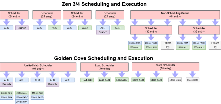
The 3d cache has to be directly at the compute cores so that each ALU can get all of the memory addresses directly from its connected AGU.
To talk to the I/O chip they would have to use the load/store.
And that is the bottleneck of the cpu.

ZEN is made to do compute on things that already are inside the cache, Cove is made to access things from outside the CPU with the biggest part of the CPU being dedicated to load store functions.

zen4_sched.png
 

bit_user

Titan
Ambassador
The 3d cache has to be directly at the compute cores so that each ALU can get all of the memory addresses directly from its connected AGU.
That's incorrect. Compute dies can access their peers' L3 cache slices, which clearly shows that the L3 needn't be located on the compute die, itself.

To talk to the I/O chip they would have to use the load/store.
Load/store is how a core interacts with the entire cache hierarchy*. Within itself and with the memory subsystem, the cache hierarchy largely transacts in terms of cachelines.

* I make an exception for loads & stores from/to uncachable memory regions, which effectively bypass the cache hierarchy (though I presume they might still make use of some underlying mechanisms).

zen4_sched.png
As for your diagram, here's how Anandtech describes the Zen 4 load/store subsystem:
"Moving on, the load/store units within each CPU core have also been given a buffer enlargement. The load queue is 22% deeper, now storing 88 loads. And according to AMD, they’ve made some unspecified changes to reduce port conflicts with their L1 data cache. Otherwise the load/store throughput remains unchanged at 3 loads and 2 stores per cycle."​

That sure sounds like it matches what's depicted of Golden Cove.
 
Last edited:

Esteban Gonzalez

Honorable
Oct 19, 2016
4
0
10,510
Hi,
Good article.
Will also be great some analisys about half the cores of the 7950x3d will not have direct access to 3d cache... this will have some impact. I bet that the 7800x3d will be far better for gaming than 7950x3d.. and for other compute needs the plain 7950x will be better than 7950x3d... I am thinking that 7950x3d is for who want both worlds...
 
That's incorrect. Compute dies can access their peers' L3 cache slices, which clearly shows that the L3 needn't be located on the compute die, itself.
My point was that you want the AGU to be able to give the ALU a mem address that is directly accessible by the ALU and not one that has to go through all of the cache hierarchy to be completed.
 

razor512

Distinguished
Jun 16, 2007
2,157
84
19,890
Cache can certainly be accessed without being on the the CCD, but the issue is how much of a performance hit takes place when it has to venture out of its own CCD to utilize that cached data, as well as how it has to work with it (e.g., is it simply copying it to a more optimal location, is it working on it directly for an extended period of time). Usually once the latency and throughput gets bad enough that it imposes more of a performance hit than simply not using it, then it will not be used.

For example, with the X3D parts, even for tasks that heavily benefit from extra cache far more than clock speed, if they are set to run on the 2nd CCD, they will not attempt to utilize the extra cache on the first CCD. What needs to be considered is even if that latency can be halved, would it be able to use that cache natively for the core, or will it have to treat it as a pseudo L4 cache where it is simply copying that data to its own local cache before doing any work with that data.
 

bit_user

Titan
Ambassador
For example, with the X3D parts, even for tasks that heavily benefit from extra cache far more than clock speed, if they are set to run on the 2nd CCD, they will not attempt to utilize the extra cache on the first CCD.
What I believe happens is that each compute die will only populate its own L3 cache slice. When fetching data, all cores must respect all L3 cache slices - to do otherwise would violate memory consistency guarantees. That's what it means to be cache-coherent.

What needs to be considered is even if that latency can be halved, would it be able to use that cache natively for the core, or will it have to treat it as a pseudo L4 cache where it is simply copying that data to its own local cache before doing any work with that data.
If you unified all L3 in the I/O die, then it could either be freely shared or remain partitioned among all the cores, in terms of who can populate it.

As for whether data is copied from L3 upon use: yes, that's how caches work. When a lower-numbered cache tier is missing the requested data, it fetches from the next higher tier. The last tier fetches it from memory. Of course, if it's sitting in a peer's L1 or L2 and it's dirty, then the dirty cacheline must get copied from there (presumably via a flush to L3).

One key difference you'll find between implementations is whether L3 is exclusive or nonexclusive of L2. In an exclusive implementation, L3 doesn't retain a cache line after it's been transferred to L2. Once the cache line is evicted by that L2 slice, then it goes (back) into L3. This makes more efficient use of die space, at the expense of more data movement. Intel switched to an exclusive L3 in Skylake, but I'm not sure about Zen.

https://en.wikipedia.org/wiki/CPU_cache#Exclusive_versus_inclusive