AMD's Future Chips & SoC's: News, Info & Rumours.

Page 20 - Seeking answers? Join the Tom's Hardware community: where nearly two million members share solutions and discuss the latest tech.


Ah, yes. Raven Ridge.

Cheers!
 

jdwii

Splendid
I think given the A12 9800 price we can assume the price will be like that on raven ridge.

Really boring product using excavator and GCN.

But i still can see the market for it i compared I3 7100 to this APU and the APU does beat it in gaming out of the box. Place holder for Raven Ridge

Watching some videos online it can even handle a decent amount of AAA titles at low-medium 720P at around 30-60fps. Better then what i had when i first got started with the integrated graphics on Intel 945 and ATI 4200 haha.


goldstone77

Distinguished
Aug 22, 2012
2,245
14
19,965


What I said was
40% frequency over say 4GHz that is 5.6GHz, or 60% lower power will land a 39/57W TDP. Those processors are going to be beast!
What GlobalFoundries said
GLOBALFOUNDRIES 7LP
"As Dan Nenni previously discussed in his GlobalFoundries 7nm and EUV Update! blog 7LP (Leading Performance) will offer a greater than 40% performance improvement relative to 14nm or greater than 60% lower power. Area scaling will be approximately 2x and the die cost reduction will be greater than 30%, with greater than 45% in target segments. Initial customer products on 7LP are expected to launch in the first half of 2018 with volume production in the second half of 2018.
oajvimprrw3z.png

GLOBALFOUNDRIES on Track to Deliver Leading-Performance 7nm FinFET Technology
Jun 13, 2017


In September 2016, GF announced plans to develop its own 7nm FinFET technology leveraging the company’s unmatched heritage of manufacturing high-performance chips. Thanks to additional improvements at both the transistor and process levels, the 7LP technology is exceeding initial performance targets and expected to deliver greater than 40 percent more processing power and twice the area scaling than the previous 14nm FinFET technology. The technology is now ready for customer designs at the company’s leading-edge Fab 8 facility in Saratoga County, N.Y.

When: September 20th 2017
Where: Hyatt Regency Santa Clara
Speaker
Michael Mendicino, Senior Director, Leading-Edge Product Management, GLOBALFOUNDRIES


1:00-1:30
Abstract
High-performance computing and premium mobile markets continue to drive adoption of leading-edge FinFET technology, and additional segments such as AR/VR, deep learning, and automotive CPU are accelerating node migration.

GF’s leading-edge product offerings are ideally suited for those needing maximum computing performance within a given power envelope and at a balanced cost. 14LPP FinFET is a complete, fully-enabled platform in high volume manufacturing with excellent yield and Performance/Power/Area (PPA). And, 7LP technology is in development with risk production next year.

It leverages the solid foundation of 14nm and delivers more than twice the logic and SRAM density, with >40% performance boost or >60% total power reduction, compared to 14nm foundry FinFET offerings. GF is planning a seamless phase-in of EUV and additional platform extensions including performance boost and automotive, similar to 14nm FinFET.

Location
Magnolia (first floor)


Greater than 40% performance improvement relative to 14nm, or greater than 60% lower power. We will have to see which direction they take it.

Edit: 7LP(LP stands for Leading-Performance not low power) if that is any indication which direction they are taking this next node.
 

juanrga

Distinguished
BANNED
Mar 19, 2013
5,278
0
17,790


And I explained you why expecting 5.6GHz for Zen2 or TDP reduction to a 39/57W TDP is nonsense.

Not only Glofo marketing team is advertising idealized percentages that don't correspond to realistic circuits*, but their claim is for the optimal range of the node, and not a constant that one can add to any frequency achievable by 14LPP.

* That is the reason why the graphic accompanying those marketing claims reported frequencies of 8 and 10GHz. They are measuring at the transistor level, without BEOL overheads and other stuff that affect real circuits.
 

goldstone77

Distinguished
Aug 22, 2012
2,245
14
19,965
AMD’s ‘Epyc’ Design Impresses, Says Canaccord; 7-Nano is Next.
Canaccord Genuity's Matthew Ramsay digs into the details of AMD's "Epyc" server chip, and likes what he finds. He's also encouraged by the company's intent to jump to a "7-nanometer" manufacturing process for its chips late next year.
ByTiernan Ray Updated Sept. 8, 2017 5:20 p.m. ET

BN-VA219_201709_P_20170908171524.png

Canaccord Genuity’s Matthew Ramsay today reiterates a Buy rating on shares of chip maker Advanced Micro Devices (AMD), and a $20 price target, after reflecting on the company’s presentation at the "Hot Chips" conference in Cupertino, California last month, and his own research on the company’s sales trends.

“Overall, while we recognize roadmap execution and competitive risks remain,” writes Ramsay, "we believe risk/reward is still tilted toward the upside."

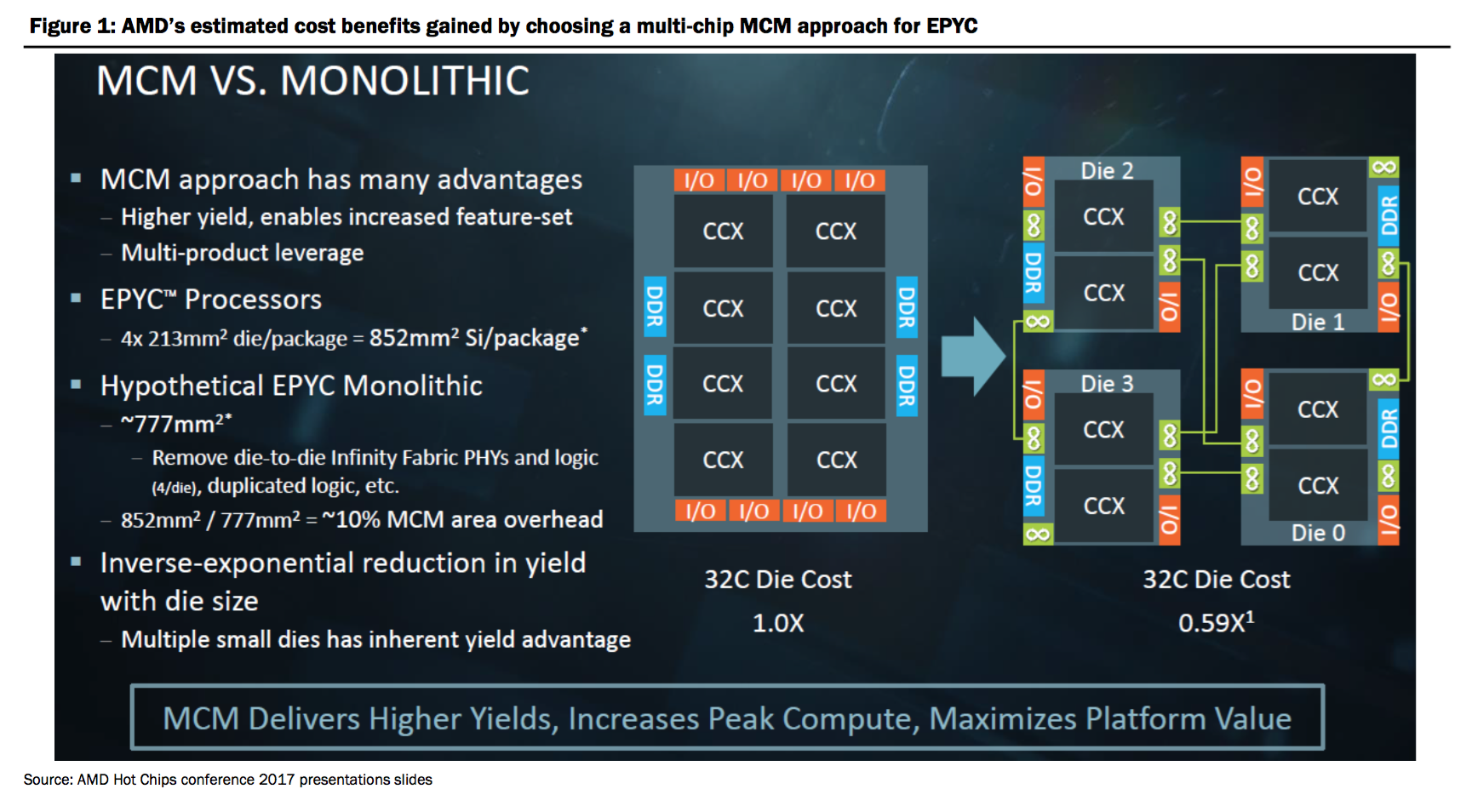
Ramsay spends a considerable amount of time talking about the company’s “Epyc” server chip. AMD made the controversial decision to string together four separate chips in place of one, as shown in the info-graphic at the top of this post.

While there may be “corner cases” where the approach is beaten by Intel’s (INTC) “Xeon” chip, Ramsay overall sees the decision as a good one on AMD’s part:

Given cost/yield realities of n- node silicon, AMD chose to design its initial EPYC server products as 4-chip multi-chip modules (MCMs) versus as single larger chips, and this has proven an area of debate in our investor conversations versus the single-die approach taken by Intel. While this design choice has many benefits including lower costs, higher yields and a simplification of the roadmap, we acknowledge there are corner cases where non-uniform memory access latency could be problematic. However, we believe essentially all high-tier software and modern OS kernels are NUMA-aware and believe AMD has only excluded initial EPYC systems from a very small subset of the server TAM through this design compromise. The benefits, however, are substantial in terms of roadmap simplicity and chip yields. In fact, as shown in Figure 1 below, AMD estimates 41% cost savings in a 4-chip 32-core package versus a single 32-core EPYC chip. In addition, important reliability availability serviceability (RAS) features are included in EPYC and leverage AMD's Infinity Fabric enhances system design flexibility and scalabliity – for instance, close integration with AMD's Radeon Instinct GPU accelerators. We believe the Hot Chips talk adds to our recent discussions with CTO Mark Papermaster (and more importantly EPYC customer endorsements) to further dispel the myth EPYC is just four desktop CPUs linked together.

While we certainly do not anticipate AMD will compete across the full breadth of Intel’s server stack or at all price points with even close to the same number of SKUs, we do believe early indications of system design (leveraging the infinity fabric) and the 14/7nm Zen core roadmaps will set price/performance points for memory/IO focused workloads such that our estimates of $1.15B in server revenue (or roughly 7% of the TAM) by 2020 are quite realistic and conservative. Additionally, a sensitivity analysis of AMD non-GAAP EPS to EPYC server market share appears in Figure 7 later in this report with 10%+ server share driving material upside to the “at least” $0.75 non-GAAP EPS target set by management.

Ramsay looks forward to chips late next year from AMD that may have smaller feature sizes of 7-nanometer, down from 14-nanometer for the current parts, which will bring a boost to performance.

“7 is the new 10,” Ramsay declares, an allusion to AMD skipping the 10-nanometer node that some chip designers are moving to:

Looking forward at the future desktop and server roadmaps from AMD, we believe 2H/18 will bring the introduction of 7nm products followed by a full year of 7nm products across the portfolio in 2019. By taking the roadmap from 14nm down to 7nm in the next generation, we believe AMD's products can have much higher performance and performance/watt versus today's 14nm Ryzen and EPYC roadmaps. Further, we anticipate these new 7nm products will compete with the 10nm roadmap from Intel. Given our view – shared by Mark Papermaster in our recent discussions – that 7nm foundry silicon is roughly equivalent to Intel's 10nm node in terms of realized performance/density/power, we believe another significant shift in the competitiveness of AMD's products versus Intel's will take place in 2018/19, leaving AMD at process node parity with Intel for the first time in well over a decade. We continue to believe investors underestimate the importance of this roadmap development for AMD's second-generation Zen-based products and primarily focus only on nearer-term results. Should AMD execute the 7nm roadmaps in 2018/19, we believe more substantial share gains could result. In addition, industry contacts indicate datacenter customers watch 7nm developments closely under NDAs and we believe AMD has already "taped out" multiple 7nm chips with positive early indications.

Ramsay also offers a couple thoughts about AMD’s “Vega” graphics chip, which competes with parts from Nvidia (NVDA). He writes that he was “disappointed,” if slightly, with "the performance and perf/watt metrics” of the GPUs.

However, "we do believe Vega increases AMD's higher-tier SAM and crypto-currency demand should help drive solid graphics sales growth near-term and until 7nm Navi GPUs launch in 2018."

Ramsay in addition offers some feedback on sales trends for AMD’s “Ryzen” chips for desktop PCs, trends he finds favorable:

Our checks indicate solid and continued gradual share gains for AMD Ryzen CPU chips across all five top OEMs (Dell, HP, Lenovo, Asus, Acer) – including important Alienware systems from Dell’s gaming division on AMD Threadripper CPUs. In addition, AMD recently launched Ryzen Pro enterprise-focused SKUs with Dell, HP and Lenovo for 2H/17. Given the much more competitive performance and cost structure of Zen-based Ryzen chipsets versus Intel, we estimate AMD will grow its PC CPU business by roughly 50% in 2017 Y/Y (granted versus very poor results in 2016) based mostly on Ryzen desktop products and also that new Zen-based 14nm products yield a gross margin roughly 10-20 points higher than previous 28nm products depending on product SKU.

Ramsay offers one last though about financials: Estimates may be too high for the end of this year and the beginning of next year, he thinks:

While we raise our Q3/17 estimates slightly and remain well above consensus for 2H/18 and for long-term AMD revenue and earnings estimates, we believe consensus estimates for Q4/17 and potentially Q1/18 may be slightly too aggressive given tougher gaming console compares and seasonality combined with an EYPC sales ramp we anticipate will accelerate meaningfully during 1H/18 versus sooner given the server adoption cycle and strong early traction with customers and partners.

Ramsay is modeling Q4 sales this year of $1.32 billion, and EPS of 2 cents per share. The Street is modeling $1.333 billion and 4 cents per share.

For Q1, he models AMD making $1.148 billion and losing 4 cents per share. That compares to consensus for $1.19 billion and 2 cents per share.
 

goldstone77

Distinguished
Aug 22, 2012
2,245
14
19,965
HW News: X399 Outstripping X299, PCIe 5.0, 1900X CCXs
Gamers Nexus
Published on Sep 7, 2017
Talking about this last week's hardware news, including X399 vs. X299 sales, PCIe 4.0 & 5.0, and new peripherals.

[video="https://www.youtube.com/watch?v=3616WecsCBM&ab_channel=GamersNexus"][/video]
Speaking with vendors the word on the street is that looking at X299 vs. X399 the venders with whom we have spoken said that the first few days to the first week, depending on which vendor, of sales of the X399 products, related products surpassed the first month of Intel X299 products sales from those same vendors, not retailers, but actual manufacturers.
 

8350rocks

Distinguished


By the way, that volume production in 2018 bit is referring to Zen2 products.
 

jdwii

Splendid


Given that GPU division and CPU division are completely separate i'm not so sure.

But analysis already say 7nm GF is about as good as Intel's 10nm

I mean at this point they are all basically within each other that the architecture itself matters more.


You give the glass half empty view, I'll give the glass half full: capacity.

I'm sure AMD has good faith in Zen v2 so they might be securing good initial capacity for it and trying to move as much as possible to TSMC so they can use a node tuned differently for Navi, plus secure more plant capacity.

How many lines will 7nm use from GloFo? Only Dresden?

Cheers!
 

juanrga

Distinguished
BANNED
Mar 19, 2013
5,278
0
17,790


What a piece of marketing lies!

(i) They claim four records, but what they did was to count the same twice. They count the benchmark scores for two sockets and then consider the same benchmarks but for only one socket. LOL

(ii) What records? 1P EPYC does 1200 and 943, Sun servers did 1200 and 832 in 2015

https://blogs.oracle.com/bestperf/sparc-t7-1-delivers-1-chip-world-records-for-spec-cpu2006-rate-benchmarks

More about 'records' below

(iii) They compared fastest 32-core EPYC to older 22-core Broadwell Xeons, which aren't even the fastest Broadwell Xeons available.

(iv) The result just demonstrates that EPYC scaling is disastrous. With 45% moar cores, AMD only scores 25% higher in SPECint than older Broadwell.

(v) Skylake Xeons are much faster than Broadwell Xeons and beat EPYC despite lower core count

Skylake-SP actually scores about 1.38X higher than Naples on GCC. It's 1.58X higher on a per-core basis.

https://www.realworldtech.com/forum/?threadid=169894&curpostid=170012

2P EPYC scores 2360 in specint. 2P SKL does 2930.
 

juanrga

Distinguished
BANNED
Mar 19, 2013
5,278
0
17,790


Only some posts ago, certain people tried to convince me that Navi used Glofo 7nm, because it was the best node. Now I am already reading excuses on how AMD may want to use TSMC 7nm for Navi instead.
 

goldstone77

Distinguished
Aug 22, 2012
2,245
14
19,965


If you remember correctly I mentioned(on more than one occasion) that AMD redefined agreement with GlobalFoundries to use any foundry including TSMC, which Lisa Su made sure to emphasize during the investor day presentation. If CoWoS (chip-on-wafer-on-substrate) is better for AMD GPU's why not utilize it. Having more than one foundry competing for your business is just smart!
 

juanrga

Distinguished
BANNED
Mar 19, 2013
5,278
0
17,790


And my point has been ignored...

Also this amended WSA has an economic cost to AMD. AMD has to pay twice: one to Glofo for not using the wafers and another to TSMC for using the wafers. That doesn't look very smart.


You also ignored mine. Capacity. AFAIK AMD only has to pay up if they don't fill up the lines.

Cheers!
 

juanrga

Distinguished
BANNED
Mar 19, 2013
5,278
0
17,790


AMD already did paid Glofo $335 millions to change the WSA, plus AMD agreed to "Make quarterly payments to GF beginning in 2017 based on the volume of certain wafers purchased from another wafer foundry."

Nowhere it says that payments are based in Glofo capacity. Payments are based in number of waffers purchased from other companies.

http://techreport.com/news/30600/amd-takes-a-335m-one-time-charge-for-more-sourcing-flexibility
 

goldstone77

Distinguished
Aug 22, 2012
2,245
14
19,965
AMD Amends GlobalFoundries Wafer Supply Agreement Through 2020, Gaining New Flexibility & New Costs
by Ryan Smith on September 1, 2016 6:00 AM EST

This evening AMD has announced that they have updated their long-standing wafer supply agreement with fab parter GlobalFoundries. The new agreement, which makes some notable alterations to wafer order numbers and how the parties are compensated, covers wafer sales between the two parties through 2020.

As a bit of background here, of the many important and long-term consequences of AMD’s 2008 spin-off of their foundry business into what has become GlobalFoundries, perhaps the most significant is the Wafer Supply Agreement (WSA). As part of the plan for separating chip design and chip fabbing, AMD inked an agreement with GlobalFoundries that setup a basic framework for how many wafers AMD would buy. This essentially ensured that AMD would remain a long-term customer and GlobalFoundries a long-term supplier through the lifetime of the agreement.

The overall WSA agreement is set to run through 2024. However throughout the lifetime of the agreement, AMD and GlobalFoundries have amended it several times to account for changing market conditions, AMD’s manufacturing needs, and GlobalFoundries own manufacturing plans. Traditionally this has been a near-yearly event – the WSA has been amended 5 times before today – however for this 6th amendment, AMD and GlobalFoundries have inked a much longer 5-year amendment that will take them through 2020.
WSA3.png

So what’s new with the latest amendment? The fundamentals have not changed; the WSA continues to ensure that AMD purchases a significant number of wafers from GlobalFoundries. However the number of wafers and how those are priced has been laid out in a different manner than previous agreements. On the pricing front, the new agreement sets fixed prices for the rest of 2016. Prices beyond that are not (yet) fixed, but according to AMD there is now a framework for how those prices are determined.
WSA4.png

So what’s new with the latest amendment? The fundamentals have not changed; the WSA continues to ensure that AMD purchases a significant number of wafers from GlobalFoundries. However the number of wafers and how those are priced has been laid out in a different manner than previous agreements. On the pricing front, the new agreement sets fixed prices for the rest of 2016. Prices beyond that are not (yet) fixed, but according to AMD there is now a framework for how those prices are determined.

This flexibility comes at a cost though. Not unlike past years where AMD has paid GlobalFoundries a penalty under take-or-pay, AMD will be paying the foundry for this new flexibility. GlobalFoundries will be receiving a $100M payment from AMD, spread out over the next 4 quarters. Meanwhile starting in 2017, AMD will also have to pay GlobalFoundries for wafers they buy from third-party foundries. This in particular is a notable change from past agreements, as AMD has never paid a penalty before in this fashion. Ultimately this means AMD could end up paying GlobalFoundries two different types of penalties: one for making a chip at another fab, and a second penalty if AMD doesn’t make their wafer target for the year with GlobalFoundries.
WSA5.png

Along with all of the above, in exchange for the latest agreement AMD is making one more payment in the form of a stock warrant. The warrant itself comes with certain stipulations, but in essence AMD is issuing a warrant to GlobalFoundries’ owner Mubadala Development Company as an additional form of compensation. The warrant will give Mubadala the option to buy up to 75 million AMD shares at a currently below-market price of $5.98/share, so long as they continue to own less than 20% of AMD. AMD is valuing the warrant at $235 million, which will bring the total one-time-costs of the latest agreement to $335M.
WSA6.png

As for AMD’s total wafer buys, the company also announced that by the end of 2016 AMD will have purchased $650 million in wafers from GlobalFoundries for the year. This is composed of $155M in wafer buys in Q1 under the old amendment, and a further $495M in Q2 through Q4 under the new agreement.

Looking at the broader picture, AMD isn’t saying how future products are being divided up among GlobalFoundries and third-party fabs, only that they’ve entered into this agreement based on what they project their future needs will be. So whether this is for CPUs, APUs, GPUs, semi-custom, or all of the above remains to be seen.

However it is interesting to note that GlobalFoundries will not be doing a 10nm process – the company is going to jump from 14nm to 7nm – so if AMD does decide to fab anything at 10nm, then it will have to be with a third-party fab. At the same time though it’s not clear how long of a shelf-life 10nm will have – there are signs it may be a short-lived process before 7nm is ready – so the lack of a 10nm process may not have much of an impact for AMD. Regardless, AMD and GlobalFoundries will be collaborating on the development of 7nm tech, so it’s clear that GlobalFoundries is expected to remain as a leading-edge supplier for AMD wafers for the next 5 years.


Looking at the broader picture, AMD isn’t saying how future products are being divided up among GlobalFoundries and third-party fabs, only that they’ve entered into this agreement based on what they project their future needs will be. So whether this is for CPUs, APUs, GPUs, semi-custom, or all of the above remains to be seen.

So, we don't know the details of the terms to understand the impact, if any, for different product lines.


ROFL. So, according to you, AMD should wait until GloFo has capacity to build whatever they can and keep themselves from selling products on whatever node they have? What they signed is *precisely* for them to avoid that scenario.

You really have a weird understanding of business, Juan.

Cheers!
 

jdwii

Splendid


I believe what he is saying is that they would have to pay global foundries if they used TSMC over the contract not that they should chose this or that.


I do understand that as well. So, you're also saying AMD should not seek extra capacity elsewhere if GloFo can't provide and keep themselves from selling more because of the agreement?

At the end of the day it's just about what is more profitable here. Nothing so stupidly complex to understand. If they make money by seeking another foundry for a product, even with the need to pay GloFo, why not?

Cheers!
 

juanrga

Distinguished
BANNED
Mar 19, 2013
5,278
0
17,790


LOL. What a way to ignore what I wrote!!

I simply mentioned that AMD paid a fixed $335 million tax to Glofo for breaking the rules of the WSA than AMD signed in the past, and I mentioned that AMD will do a second variable payment as function of the number of orders made on TSMC/Samsung foundries. Your former claim that


is not true, because AMD already paid $335 millions independently of the production.

It is evident to me that AMD renegotiated the WSA because Glofo 7nm is not the panacea that some try to sell us. In fact I guess that Glofo 7nm is not suitable for GPUs, and that AMD want to do GPUs on TSMC.


Because they had a fix wafer agreement that, depending on extra capacity would need a renegotiation of the price? I do get that I did not remember correctly the terms, but it still doesn't justify why you think the only reason is that GloFo won't be able to produce a node in 7nm that won't satisfy the GPUs. Like I said, I just gave the glass half full appraisal.

So, again, you think AMD is better off just depending on GloFo's capacity (as well as quality of nodes)? Let me re-phrase. From what I understand you're trying to get at, your argument goes along the lines of: "AMD can't escape GloFo, therefore the only reason is because their node is crap". Well, I'm telling you: "no, not really".

Cheers!

EDIT: Typos.
 

juanrga

Distinguished
BANNED
Mar 19, 2013
5,278
0
17,790


It isn't related to capacity. If Glofo production line fas entirely filled with AMD products and AMD needs more production, then AMD would simply order the rest in other foundries, and would not take any penalty because Glofo would be receiving the minimum wafer orders stated in the previous WSA.

The only logical reason why AMD renegotiated the WSA, and is paying two penalties to Glofo for breaking the previously signed agreement is because the Glofo process node doesn't have the quality required. I can infer that Glofo 7LP, which is a process derived from IBM foundry technology, is not a valid process for making GPUs¹ and I can perfectly understand that AMD would want to use TSMC for Navi.

Guess what? the rumor is that AMD want do Navi on TSMC 7nm

http://www.digitimes.com/news/a20170908PD210.html

Footnote:

¹ IBM foundry never make GPUs, and former Glofo nodes based in IBM technology, weren't used for GPUs. E.g. AMD didn't make GPUs in 32PDSOI process; AMD used TSMC for 32nm GPUs.
 

jdwii

Splendid


No i'm not if anything i wish they would use TSMC i just don't think they can since they would have to pay global foundry's extra
 

TRENDING THREADS