Just finishing up here at work so this'll be my last post for a bit, check in later.
JAYDEEJOHN :
They added that about the x2 later. This is how I see it then. Im thinking theyll still go for a higher shader clock, and didnt we see better power/performance going from 2xxx to the 3xxx series?
Yes that's true, but they also went from a problematic TSMC 80nm HS fab to the luckily very stable 55nm fab, which jumped a full node in the process (move node and optical shrink bypassing 65nm), and this time around you'd be going from a stable 55nm process to an unknown 45/40nm fab. May or may not be better/same/worse. I wouldn't count on the same power/heat reductions we got from the HD2K-3K
Im thinking well see a repeat of this again. The speed of the shaders will cause some heat issues, but since it isnt a huge increase in shaders like we saw going from 2xxx to 3xxx, itll be more manageable.
I agree somewhat, it's definitely less than I originally thought (+12.5% vs +150%) , but I'd say adding 12.5% and then increasing speed by at least that amount (go from 800MHz to 1GHz) would be quite a burden.
Besides, it gets to a certain point where your flogging a dead horse using the same arch. Just like we saw very little improvement with the G280, Im thinking the same for the 5xxx series other than the shader clocks
Definitely, but the question is how you change. I'm curious about their scaling if they're stil resorting to amplification of compoents and not exploiting raw efficiencies.
I think the HD4K is a very weird beast though because as a single chip it's very cost focused, but heat and temp wise it's not better than the GTX which is that big single chip solution. When it came out we were all thinking, yeah nV's in big trouble, because you'd never put that much heat & power draw on a single card, but oie, it's actually nearly the same as the HD4K, and it's not the power/heat that's keeping them from making a GX2 it's the yields & cost (especially of a complex board).
I don't know I guess, I'm a little bitter at the fact that this loses them the modular option of laptops solutions, in which there's just as equally no freakin' way they're plopping an HD48xx in anywhere near its current form in a laptop. And that to me was where another benefit of the modular design lay, and it's lost due to the power/heat issues.
There's no arguing that increasing so many components by 2.5X without increasing the power consumption by much more than 25% is an impressive feat with is consuming less than the HD2900XT. However it does limit modular designs greatly, where there's little benefit to an X2 when running them in QuadFire mode yields you over 500W of actually draw from the cards alone, versus less from 2 GTX in SLi, and with the still yet to be refined Tri & Quad scaling I'm not sure that Quadfire would be as attractive as GTX SLi in many cases. Anywhoo, still early for any of this, just my major reservation sofar, which may admittedly be jumping the gun a bit.
ATI come with 45nm While nVIDIA Still in 65nm?
nV will be 55nm by the fall with the GTX refresh.
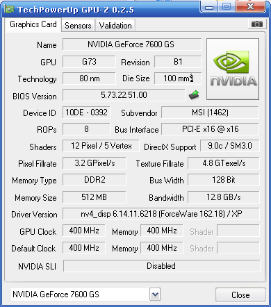
I have MSI NX 7600GS and i can't OC it more then 433MHz (normal=400MHz)
because the 80nm GPU !
even Geforce 8600 stil use 80nm article .
I though the GF7600GS was 90nm only the GF7650 was to be 80nm, but then again there's lotsa naming monkey business.
Anywhoo, 45nm doesn't guarantee higher OCs anymore than TSMC's overheating 80nmHS did for the R600. One would hope it offers some more headroom, but that depends on the other factors like power & heat as well as a stable process node.


")