I was wondering about the rumor that the i5 and i3 processors are really just i7 processors that came off the assembly line defective in the areas not used by the lower chips. In fact, the i5 and i3 designs could have been completely based on reduced or non-existent features of the i7 chip.
Flawed Intel processors
- Thread starter ddrambo
- Start date
-
- Tags
- Power Supplies Product Support
You are using an out of date browser. It may not display this or other websites correctly.
You should upgrade or use an alternative browser.
You should upgrade or use an alternative browser.
Solution
Nope, i3/i5 Duals are 32nm Clarkdales with only 2 cores on the die, while i5 7XX/i7 8XX quads are 45nm Lynnsfields with 4 cores on the die.
Intel does do chip-harvesting (thats whats it called) though, for example disabling the L3 in the Pentum GXXXX series. You could also consider the i5-750 as a harvested Lynnfield, as HT is disabled, but that is more likely a result of binning.
Intel does do chip-harvesting (thats whats it called) though, for example disabling the L3 in the Pentum GXXXX series. You could also consider the i5-750 as a harvested Lynnfield, as HT is disabled, but that is more likely a result of binning.
Timop
Distinguished
- Feb 27, 2010
- 3,070
- 0
- 21,160


Nope, i3/i5 Duals are 32nm Clarkdales with only 2 cores on the die, while i5 7XX/i7 8XX quads are 45nm Lynnsfields with 4 cores on the die.
Intel does do chip-harvesting (thats whats it called) though, for example disabling the L3 in the Pentum GXXXX series. You could also consider the i5-750 as a harvested Lynnfield, as HT is disabled, but that is more likely a result of binning.
Intel does do chip-harvesting (thats whats it called) though, for example disabling the L3 in the Pentum GXXXX series. You could also consider the i5-750 as a harvested Lynnfield, as HT is disabled, but that is more likely a result of binning.
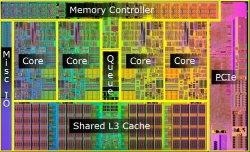
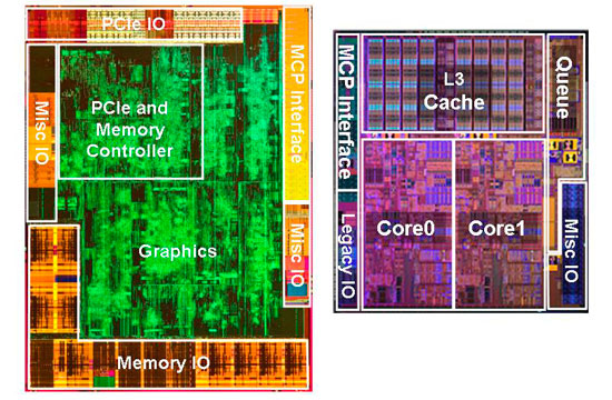
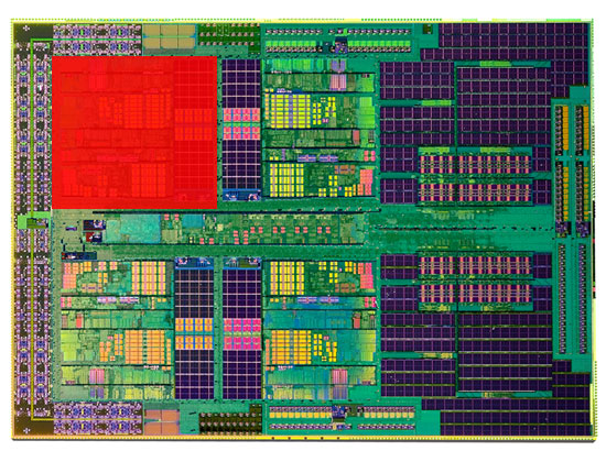
I must say that the diagrams presented by wr2 are compelling, but if you look closer you'll notice some similarities and obvious confusing details. For example, the smaller i5 clarkdale is very much like a section of the i7. The coloration is obviously artificial and added to identify different sections. The i3 clarkdale is totally different and doesn't make sense at all when compared to the others. It's as though they took an actual photo of the active chip with infrared film, then colorized it like the others. Someone with photoshop could have easily created all of them by moving blocks around to create the i7 and i5 diagrams, but actual photos in block form in the i3. I can't believe that the difference between the i3 core and the others is actually that large using the same die structure. Ironically, the blurred effect of the i3 structure confuses the comparison for some reason because this was intentional.
I initially noticed when I read about the i7 and i5 that the i5 had the same features as the i7, but some of them were 'turned off', which led me to research further. If you do this same research for the i3 you find the same thing, except I noticed that some of the features of the i3 which were not mentioned as being in the i5 or i7 were in fact a part of those other chips when I dug deeper into other descriptions of them all. So other than the apparent size difference and the attempt to confuse you with different parsing of the block positions, and apparent bluriness, these could all be the same chip set with features turn off or disabled or non-functional, however you wish to look at it. There is no proof here or in anything else I've read that they aren't the same, except in the minds of those who wish to believe what Intel tells them.
I initially noticed when I read about the i7 and i5 that the i5 had the same features as the i7, but some of them were 'turned off', which led me to research further. If you do this same research for the i3 you find the same thing, except I noticed that some of the features of the i3 which were not mentioned as being in the i5 or i7 were in fact a part of those other chips when I dug deeper into other descriptions of them all. So other than the apparent size difference and the attempt to confuse you with different parsing of the block positions, and apparent bluriness, these could all be the same chip set with features turn off or disabled or non-functional, however you wish to look at it. There is no proof here or in anything else I've read that they aren't the same, except in the minds of those who wish to believe what Intel tells them.
jimmysmitty
Champion
- Oct 5, 2007
- 21,595
- 595
- 59,140


ddrambo :
I must say that the diagrams presented by wr2 are compelling, but if you look closer you'll notice some similarities and obvious confusing details. For example, the smaller i5 clarkdale is very much like a section of the i7. The coloration is obviously artificial and added to identify different sections. The i3 clarkdale is totally different and doesn't make sense at all when compared to the others. It's as though they took an actual photo of the active chip with infrared film, then colorized it like the others. Someone with photoshop could have easily created all of them by moving blocks around to create the i7 and i5 diagrams, but actual photos in block form in the i3. I can't believe that the difference between the i3 core and the others is actually that large using the same die structure. Ironically, the blurred effect of the i3 structure confuses the comparison for some reason because this was intentional.
I initially noticed when I read about the i7 and i5 that the i5 had the same features as the i7, but some of them were 'turned off', which led me to research further. If you do this same research for the i3 you find the same thing, except I noticed that some of the features of the i3 which were not mentioned as being in the i5 or i7 were in fact a part of those other chips when I dug deeper into other descriptions of them all. So other than the apparent size difference and the attempt to confuse you with different parsing of the block positions, and apparent bluriness, these could all be the same chip set with features turn off or disabled or non-functional, however you wish to look at it. There is no proof here or in anything else I've read that they aren't the same, except in the minds of those who wish to believe what Intel tells them.
I initially noticed when I read about the i7 and i5 that the i5 had the same features as the i7, but some of them were 'turned off', which led me to research further. If you do this same research for the i3 you find the same thing, except I noticed that some of the features of the i3 which were not mentioned as being in the i5 or i7 were in fact a part of those other chips when I dug deeper into other descriptions of them all. So other than the apparent size difference and the attempt to confuse you with different parsing of the block positions, and apparent bluriness, these could all be the same chip set with features turn off or disabled or non-functional, however you wish to look at it. There is no proof here or in anything else I've read that they aren't the same, except in the minds of those who wish to believe what Intel tells them.
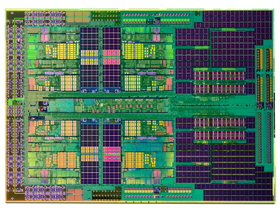
The reason the details look the same is because the Core i3/i5 is a die shrink of Nehalem. So it uses the same core technology and cache technology only at a smaller process. How you could get that they are just defective 45nm Core i7s is beyond me. I don't think its possible to turn a 45nm chip into a 32nm chip.
As I said, Westmere (Core i3/i5) is the same chip as Nehalem (Core i5/i7) in terms of the design and features they could add on. But they are a different process. There are no 32nm quad core i7s. Hell there are no triple core i7s.
cjl
Splendid
- Jun 18, 2008
- 7,676
- 0
- 31,160

ddrambo :
I must say that the diagrams presented by wr2 are compelling, but if you look closer you'll notice some similarities and obvious confusing details. For example, the smaller i5 clarkdale is very much like a section of the i7. The coloration is obviously artificial and added to identify different sections. The i3 clarkdale is totally different and doesn't make sense at all when compared to the others. It's as though they took an actual photo of the active chip with infrared film, then colorized it like the others. Someone with photoshop could have easily created all of them by moving blocks around to create the i7 and i5 diagrams, but actual photos in block form in the i3. I can't believe that the difference between the i3 core and the others is actually that large using the same die structure. Ironically, the blurred effect of the i3 structure confuses the comparison for some reason because this was intentional.
I initially noticed when I read about the i7 and i5 that the i5 had the same features as the i7, but some of them were 'turned off', which led me to research further. If you do this same research for the i3 you find the same thing, except I noticed that some of the features of the i3 which were not mentioned as being in the i5 or i7 were in fact a part of those other chips when I dug deeper into other descriptions of them all. So other than the apparent size difference and the attempt to confuse you with different parsing of the block positions, and apparent bluriness, these could all be the same chip set with features turn off or disabled or non-functional, however you wish to look at it. There is no proof here or in anything else I've read that they aren't the same, except in the minds of those who wish to believe what Intel tells them.
I initially noticed when I read about the i7 and i5 that the i5 had the same features as the i7, but some of them were 'turned off', which led me to research further. If you do this same research for the i3 you find the same thing, except I noticed that some of the features of the i3 which were not mentioned as being in the i5 or i7 were in fact a part of those other chips when I dug deeper into other descriptions of them all. So other than the apparent size difference and the attempt to confuse you with different parsing of the block positions, and apparent bluriness, these could all be the same chip set with features turn off or disabled or non-functional, however you wish to look at it. There is no proof here or in anything else I've read that they aren't the same, except in the minds of those who wish to believe what Intel tells them.
The i3 and i5 clarkdales look exactly the same - you're misinterpreting the photo. The die on the left is the graphics die (45nm) and the die on the right is the clarkdale CPU die (32nm), both of which are put together into an MCM to make a clarkdale chip with graphics.
Oh, and as for the CPU die looking like a Lynnfield/Bloomfield section, that's not all that surprising. The core logic is similar, as is the core:cache ratio, so they should look similar. They're made on different processes though (Lynnfield/Bloomfield are on 45nm, clarkdale is on 32nm), so even though they look the same, the design is significantly different. i3 and i5 processors are close to the same (just with different clocks and feature sets), and the i5-750 and i7-800 series are the same way. There's a tremendous difference in dies between the i3/i5 series and the i5-750/i7-800 series though.
WR2
Polypheme
- Nov 18, 2005
- 27,923
- 6
- 64,715


ddrambo :
There is no proof here or in anything else I've read that they aren't the same, except in the minds of those who wish to believe what Intel tells them.
AMD Phenom II X2 555 BE AM3
AMD Phenom II X4 955 BE AM3
WR2
Polypheme
- Nov 18, 2005
- 27,923
- 6
- 64,715
TRENDING THREADS
-
Question No POST on new AM5 build - - - and the CPU & DRAM lights are on ?
- Started by Uknownflowet
- Replies: 13
-

-
 Discussion Feasibility & feedback on a compact, high-density 20-NVMe JBOF Enclosure ?
- Started by NOR1NCO
- Replies: 1
-

-
-
Latest posts
-
 Question Can someone from actual use experience (monitor screen cleaning)
- Latest: Roland Of Gilead
-

-

-

-

Space.com is part of Future plc, an international media group and leading digital publisher. Visit our corporate site.
© Future Publishing Limited Quay House, The Ambury, Bath BA1 1UA. All rights reserved. England and Wales company registration number 2008885.
 Twitter