- Nov 21, 2018
- 27,170
- 1,263
- 44,560


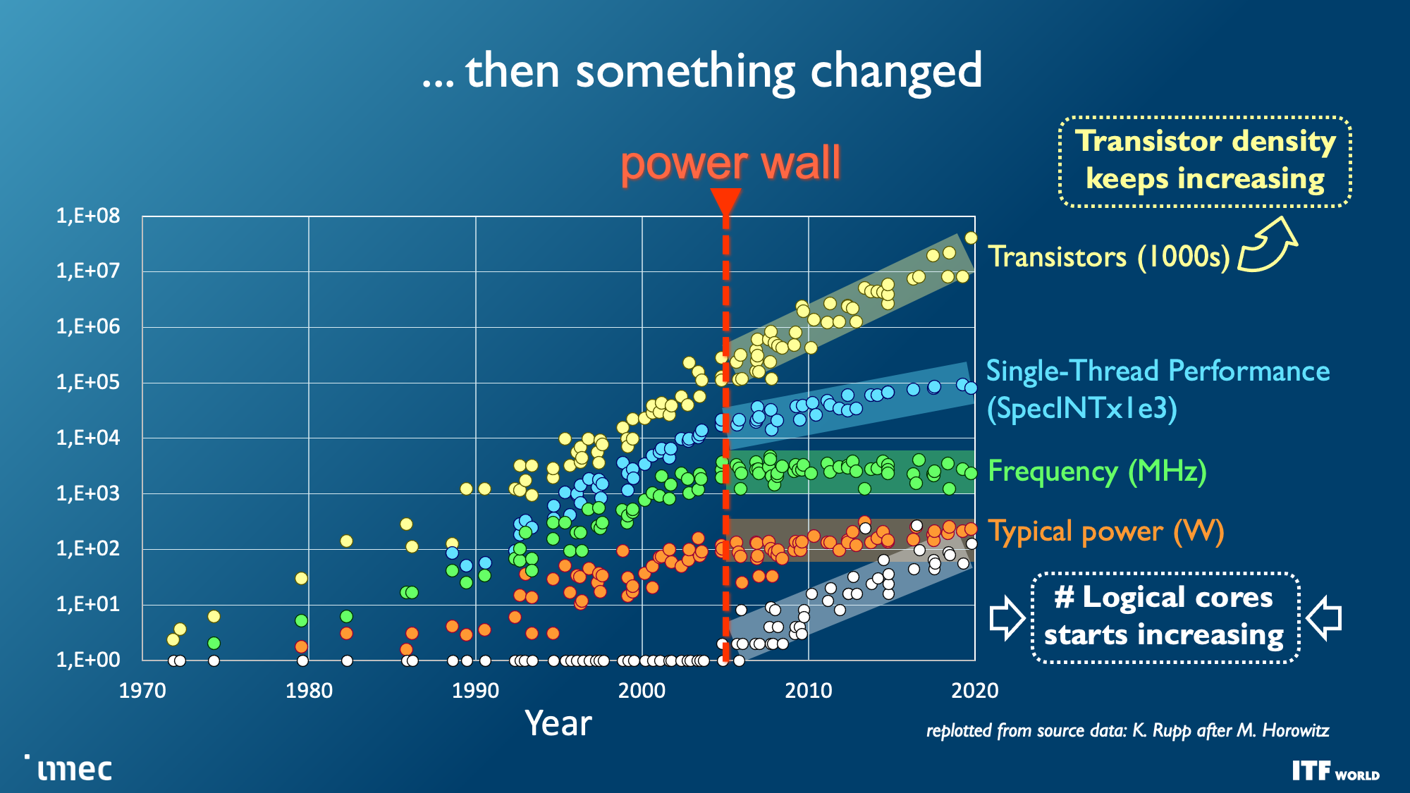
Imec, the most advanced semiconductor research firm in the world, recently shared its silicon and transistor roadmap at its ITF World summit in Antwerp, Belgium.
Imec Reveals Sub-1nm Transistor Roadmap, 3D-Stacked CMOS 2.0 Plans : Read more
Imec Reveals Sub-1nm Transistor Roadmap, 3D-Stacked CMOS 2.0 Plans : Read more


")
 Twitter