Intel to describe benefits of PowerVia backside PDN with 4nm-class test chip.
Intel to Show Off E-Core-Based CPU with Backside Power Delivery : Read more
Intel to Show Off E-Core-Based CPU with Backside Power Delivery : Read more
"Backside Power Delivery", AKA Arse Power?Intel to describe benefits of PowerVia backside PDN with 4nm-class test chip.
Intel to Show Off E-Core-Based CPU with Backside Power Delivery : Read more
Definitely IFS. I think Intel would have to blow away the competition for a fair amount of time with their own designs if Apple were to give up on their own chips at this point.Arm is interested, If TSMC does not have comparative tech, Could see Intel regaining Apple as a customer, albeit as IFS in the future.
It would be about the manufacturing process not the design, ifs is made to be able to handle different designs.Definitely IFS. I think Intel would have to blow away the competition for a fair amount of time with their own designs if Apple were to give up on their own chips at this point.
A chip that will never be mass produced will show the benefits of a crucial technology.
Arm is interested, If TSMC does not have comparative tech, Could see Intel regaining Apple as a customer, albeit as IFS in the future.
Except that this is Backside Power Delivery being tested on Intel 4. That makes it a nonstandard Intel 4, which is why this is a test chip and not real product.If they're messing around with Crestmont E-cores, then maybe we'll see a Meteor Lake-N sooner than... 2025?
Yes, but it would need more cores to justify that. I think only the 8-core Alder Lake-N can really justify dual-channel DDR5. Plus, the sad reality is that Intel probably saw that 90% of their E-CPUs were being implemented with only one channel and felt it was a waste even to build-in the second channel.Give it 2 memory channels this time.
Yes, I was going to post that same link. The key difference being that TSMC will lag in this respect, for a whole ~2 years.Sounds like TSMC also has plansfor a backdoorto take it up the backside...
🤣
TSMC Outlines 2nm Plans: N2P Brings Backside Power Delivery in 2026, N2X Added To Roadmap
The short answer is that power and data are currently both routed in from the same side of the chip.Where is the power routed in current chips?
This is independent of chip-stacking. I'm not sure how much relevance it has for chip stacking (i.e. if it makes it easier, etc.), or if it's completely independent.Is this basically a chip stacking tech - with a power layer being the base ?
Referring to the % of die area that can be used for logic cells, I think. Ideally, you want 100% of die area to be consumed by cells, but routing & other constraints result in actual densities that are less. By getting power delivery "out of the way", it enables denser logic.What is cell utilization ?
You might want to re-phrase that statement.Sounds like TSMC also has plans for a backdoor...
TSMC Outlines 2nm Plans: N2P Brings Backside Power Delivery in 2026, N2X Added To Roadmap
The 100% die are utilization is "Theoretical". realistically, you still have to have some power lines going to some points on the logic area. it can't be 100%, just close.Referring to the % of die area that can be used for logic cells, I think. Ideally, you want 100% of die area to be consumed by cells, but routing & other constraints result in actual densities that are less. By getting power delivery "out of the way", it enables denser logic.
The benefit of higher density is basically to improve the cost-efficiency of the chips. Also, packing more logic in a smaller area means data has to travel shorter distances, which can translate either into higher clockspeeds or a greater amount of work being done per clock cycle.
Don't get too excited, because thermal density is becoming an increasingly limiting factor. High density is therefore most beneficial to low-power chips, like phone SoCs.
Intel keeps all the things together keeping the surface area big and easy to cool so that you can cool a 13900k with a $20 cooler without losing performance, and the mock ups of meteorlake also shows them keeping everything together despite it being based on tiles so hopes ARE high, they don't split things up into multiple very dense hot spots making the CPU terrible to cool.Don't get too excited, because thermal density is becoming an increasingly limiting factor. High density is therefore most beneficial to low-power chips, like phone SoCs.

Again, that's irrelevant because this is an article about Intel 4. And not even standard Intel 4, but a modified variant intended to evaluate their PowerVias. Please don't thread-jack to work your agenda.you can cool a 13900k with a $20 cooler
It's not irrelevant because they will have the same basic topography with everything being one big large area to cool, so the capability to cool current gen is very much relevant.Again, that's irrelevant because this is an article about Intel 4. And not even standard Intel 4, but a modified variant intended to evaluate their PowerVias. Please don't thread-jack to work your agenda.
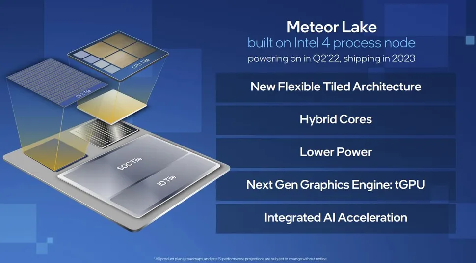
Specifically what topography are you talking about? The high-level floorplan of Meteor Lake sure isn't the same, with the CPU cores scrunched into one corner.It's not irrelevant because they will have the same basic topography with everything being one big large area to cool,

It's all packed together creating one large surface area making heat dissipation easier just as it is on the current CPUs.Specifically what topography are you talking about? The high-level floorplan of Meteor Lake sure isn't the same, with the CPU cores scrunched into one corner.

Huh? How is "packing together" supposed to be a good thing? When you have multiple hot things, you'd like to space them apart, so the heat from one can be dissipated without interference from others.It's all packed together creating one large surface area making heat dissipation easier just as it is on the current CPUs.


