
- Sep 21, 2008
- 4,568
- 10
- 23,160


Memory - Part I - "What memory is"
other content:
Part II - "What memory does"
Part III - "Evaluation and selection"
Part IV - "Tweaking and tuning"

A great deal of the information contained in this section, as well as most of the great illustrations, have been 'extracted' from "What Every Programmer Should Know About Memory" by Ulrich Drepper of RedHat, Inc.; the original PDF can be found here. I cannot recommend this document highly enough; however, it is 'aimed at' the more 'mechanical' details of memory (and especially CPU cache) access, and how to optimize these to get responsive, efficient programs; thus, contains a large amount of detail (114 pages!) that many will find mostly irrelevant... Also, if the references here to electrical measurements and terms 'draw a blank', and you'd like a bit of a primer, you can try a pass through Electrical Basics for Computers
One last comment before the start - the text contains a number of occurrences of the term “usually” and other, similar qualifiers. The technology discussed here exists in many, many variations in the real world and this discussion only addresses the most common, mainstream versions. It is rare that absolute statements can be made about any 'current' (which means 'evolving'!) technology, thus the qualifiers...
A little bit of ROM:
Before we consider 'live' RAM, for thoroughness, we need a short primer on ROM, just for background; Rom (read only memory) comes in a variety of 'flavors'. Every single computer must have ROM, as it provides the 'start-up sequencing' instructions to 'wake the CPU up', and get it into operation - these were called bootstrapping operations, after the old phrase: "pull yourself up by your bootstraps", and shortened to BootROM (now, the BIOS!) Due to this, the term for starting your computer came to be "boot up"! Originally created with their contents already programmed, they went through a number of evolutionary changes: PROM, which could be programmed once, after fabrication, UVPROM, which could be erased by exposure to short-wave ultraviolet light, and then reprogrammed; EEPROM (or E²PROM), which can be fully erased electrically; and EAROM, which can be reprogrammed bit by bit, electrically - all the way up to out current, ubiquitous FLASH memory. None of these have much to do with our topic, however, as the very first job of nearly every program contained in ROM is to copy itself to RAM, of one form or another, for execution!
What memory is, and how it works:
The following discusses hardware details at the gate level and the access protocol between the memory controller and the DRAM chips. Users will likely find this information enlightening since these details explain why RAM access works the way it does, and relates directly to the purchasers' price/perfomance decisions.
The first interesting details are centered around the question: why there are different types of RAM in the same machine? More specifically, why are there both static RAM (SRAM²) and dynamic RAM (DRAM)? The former is much faster and provides the same functionality. Why is not all RAM in a machine SRAM? The answer is, as one might expect, co$t. SRAM is much more expensive to produce and to use than DRAM. Both these cost factors are important, the second one increasing in importance more and more. To understand these differences we look at the implementation of a 'bit' of storage for both SRAM and DRAM:
Static RAM:
 shows the structure of a 6 transistor SRAM cell. The core of this cell is formed by the four transistors M1 to M4 which form two crosscoupled inverters. They have two stable states, representing 0 and 1 respectively. The state is stable as long as power on Vdd is available.
²...in other contexts SRAM might mean “synchronous RAM”.
For the following discussion it is important to note that:
■a 'cell' (bit) needs six transistors - variants with four exist, but they have disadvantages...
■maintaining the state of the cell requires constant power...
■the cell state is available for reading almost immediately once the word access line WL is raised...
■the signal is as rectangular (changing quickly between the two binary states) as other transistor-controlled signals...
■the cell state is stable, no 'refresh' cycles are needed...
Dynamic RAM:
Dynamic RAM is, in its structure, much simpler than static RAM. All it consists of is one transistor and one capacitor. (For you 'non-electronic' types - a capacitor is sort of like a tiny 'battery' - it 'holds a charge', which of course means that it can be 'charged' and 'discharged'... Just as an aside, they're not all 'tiny and inocuous'; I have water-glass-sized kilovolt electrolytics laying around whose 'discharge' can kill you!!) This huge difference in complexity of course means that it functions very differently than static RAM.
 A dynamic RAM cell keeps its state in the capacitor C. The transistor M is used to guard the access to the state. To read the state of the cell, the access line AL is raised; this either causes a current to flow on the dataline DL or not, depending on the charge in the capacitor. To write to the cell, the data line DL is appropriately set and then AL is raised for a time long enough to charge or drain the capacitor.
There are a number of complications with the design of dynamic RAM. The use of a capacitor means that reading the cell discharges the capacitor. The procedure cannot be repeated indefinitely, the capacitor must be recharged at some point. Even worse, to accommodate the huge number of cells (chips with 10 to the 9th, or more, cells are now common) the 'capacity' of the capacitor must be low (in the femto-farad range or lower). A fully charged capacitor only holds a few tens of thousands of electrons. Even though the resistance of the capacitor is high (a couple of tera-ohms), it only takes a short time for the capacity to dissipate. This problem is called “leakage”.
This leakage is why a DRAM cell must be constantly refreshed. For most DRAM chips these days this refresh must happen every 64μs, or oftener. During the refresh cycle no access to the memory is possible since a refresh is simply a memory read operation where the result is discarded. For some workloads this overhead might stall up to 50% of the memory accesses.
A second problem resulting from the tiny charge is that the information read from the cell is not directly usable. The data line must be connected to a sense amplifier which can distinguish between a stored 0 or 1 over the whole range of charges which still have to count as 1.
A third problem is that reading a cell causes the charge of the capacitor to be depleted. This means every read operation must be followed by an operation to recharge the capacitor. This is done automatically by feeding the output of the sense amplifier back into the capacitor. It does mean, though, the reading of memory content requires additional energy and, more importantly, time.
A fourth problem is that charging and draining a capacitor is not instantaneous. The signals received by the sense amplifier are not 'rectangular', so a conservative estimate as to when the output of the cell is usable has to be used. The formulas for charging and discharging a capacitor are:

This means it takes some time (determined by the capacity C and resistance R) for the capacitor to be charged and discharged. It also means that the current which can be detected by the sense amplifiers is not immediately available. Figure 2.6 shows the charge and discharge curves:
 The X–axis is measured in units of RC (resistance multiplied by capacitance) which is a unit of time. Unlike the static RAM /CASe where the output is immediately available when the word access line is raised, it will always take a bit of time until the capacitor discharges sufficiently. This delay severely limits how fast DRAM can be. If there is one concept I want you to 'take away' from this section, this it: underlying DRAM operation are physical processes that take finite, calculable amounts of time!!
The simple approach has its advantages, too. The main advantage is size. The chip 'real estate' needed for one DRAM cell is many times smaller than that of an SRAM cell. The SRAM cells also need individual power for the transistors maintaining the state. The structure of the DRAM cell is also tidier and more regular, which means packing many of them close together on a die is simpler. Overall, the (quite dramatic) difference in cost wins. Except in specialized hardware – network routers, for example – we have to live with main memory which is based on DRAM.
■a 'cell' (bit) needs one transistor, but depends upon a capacitor, whose charge/discharge take time...
■maintaining the state of the cell requires periodic 'refreshing' of its state...
■the cell state is available for reading only through/after discharge/amplification...
■the signal/content is a 'curve' (changing less quickly between the two binary states) compared with 'rectangular' transistor-controlled signals...
Next, we need to look into a few more details of the actual use of DRAM cells.
DRAM organization and access:
■Multiplexing
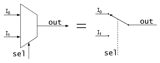
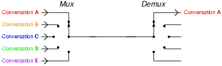
No explanation of 'what's going on with' your RAM can be made without a preliminary, cursory explanation of the use of 'multiplexing'. Multiplexing, simply described, is a means of using a limited number of transmission means (board signal traces, connector pins, cables' individual wires, connecting elements inside a chip...) to transmit a larger number of actual signals. In its simplest form, it can be shown as a 'gating' mechanism that is functionally equivalent to a two-pole switch:
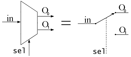
In more complex forms, any number of signals, on any number of transmission lines, can be multiplexed ('MUXed', to geeks - the corresponding 'decode' is to 'DEMUX'):
A program selects a memory location using a 'virtual address' - the CPU 'translates' this into a physical address, and finally the memory controller selects the RAM chip and cells corresponding to that address. To select the individual memory cell on the RAM chip, parts of the physical address are passed on in the form of a number of electrical address lines.
It's impractical to address memory locations individually from the memory controller: 4GB of RAM would require 2-to-the-32nd address lines (4,294,967,296!). Instead, the address is 'passed' encoded as a binary number using a smaller set of address lines. The address passed to the DRAM chip this way must be demultiplexed first. A demultiplexer with 'N' address lines must have '2N' output lines. These output lines can be used to select the memory cell. Using this direct approach is no big problem for chips with small capacities.
But, if the number of cells grows, this approach is not suitable - 1Gbit capacity would require 30 address lines and 230 select lines. The size (and co$t) of a demultiplexer increases exponentially with the number of input lines when speed is not to be sacrificed. Even more importantly, transmitting 30 impulses on the address lines synchronously is much harder (and, again, more co$tly!) than transmitting “only” 15 impulses. Fewer lines have to be laid out at exactly the same length (or 'timed' exactly)...
■/RAS and /CAS
 - a DRAM chip at a very 'high level'... The cells are organized in rows and columns. They could all be aligned in one row, but then the chip would need a huge demultiplexer. With the 'array' approach the design can get by with one demultiplexer and one multiplexer of half the size. This is a huge saving on all fronts. In the example, the address lines a0 and a1 through the row address selection (/RAS) demultiplexer select the address lines of a whole row of cells. When reading, the content of all cells is thus made available to the column address selection (/CAS) multiplexer. Based on the address lines a2 and a3, the content of one column is then made available to the data pin of the chip. This happens many times in parallel, on a number of chips, to produce a total number of bits corresponding to the width of the data bus.
For writing, the new cell value is put on the data bus and, when the cell is selected using the /RAS and /CAS,it is stored in the cell. A pretty straightforward design! There are, in reality – obviously – many more complications. There need to be specifications for how much delay there is, after the signal, before the data will be available on the data bus for reading. Again, the capacitors do not 'unload' instantaneously, as described earlier... The signal from the cell is so weak that it needs to be amplified. For writing, it must be specified how long the data must be available on the bus after the /RAS and /CAS is done to successfully store the new value in the cell (again, capacitors do not fill or drain instantaneously). These timing constants are crucial for the performance of the DRAM chip!
As mentioned, DRAM cells 'leak' their charges out over time, so that charge has to be refreshed if the DRAM is actually going to be useful as a storage device. Reading from or writing to a DRAM cell refreshes its charge, so the most common way of refreshing a DRAM is to read periodically from each cell. This isn't quite as bad as it sounds for a couple of reasons: first, you can sort of 'cheat' by only activating each row using //RAS, which is how refreshing is normally done; second, the DRAM controller takes care of scheduling the refreshes and making sure that they don't interfere with regular reads and writes. So to keep the data in DRAM chip from leaking away the DRAM controller periodically sweeps through all of the rows by cycling /RAS repeatedly and placing a series of row addresses on the address bus. A RAM grid is always a rectangle, and not a perfect square - you want fewer rows and more columns because the fewer rows you have, the less time it takes to refresh all the rows - hence the rectangular layout.
■What latency is, and why it matters:
You see, that for practical reasons, memory is 'presented to' the memory controller as a multi-dimensional array of cells ('bits'), somewhat like a spreadsheet containing many 'sheets' of rows by columns. The 'selection' of each dimension corresponds to a physical process - these are your latencies - that is, itself, dependent on physical laws. A 'W' picofarad capacitor put across an 'X' volt supply with 'Y' resistance, takes 'Z' amount of time to 'charge' to 'X' volts! You can make it slower, but you can never make it any faster...
We will not delve here (for brevity, which, BTW, I see I'm already not doing too good at[:isamuelson:6]!) into the further physical organization of these arrays: 'chips' vs 'ranks/banks', 'sides', and how the on-DIMM memory controller physically 'handles' these elements - suffice it to say that there is low-level complexity, and at every step, each level takes real, physical time!

> Next: Part II - "What memory does"
other content:
Part II - "What memory does"
Part III - "Evaluation and selection"
Part IV - "Tweaking and tuning"
A great deal of the information contained in this section, as well as most of the great illustrations, have been 'extracted' from "What Every Programmer Should Know About Memory" by Ulrich Drepper of RedHat, Inc.; the original PDF can be found here. I cannot recommend this document highly enough; however, it is 'aimed at' the more 'mechanical' details of memory (and especially CPU cache) access, and how to optimize these to get responsive, efficient programs; thus, contains a large amount of detail (114 pages!) that many will find mostly irrelevant... Also, if the references here to electrical measurements and terms 'draw a blank', and you'd like a bit of a primer, you can try a pass through Electrical Basics for Computers
One last comment before the start - the text contains a number of occurrences of the term “usually” and other, similar qualifiers. The technology discussed here exists in many, many variations in the real world and this discussion only addresses the most common, mainstream versions. It is rare that absolute statements can be made about any 'current' (which means 'evolving'!) technology, thus the qualifiers...
A little bit of ROM:
Before we consider 'live' RAM, for thoroughness, we need a short primer on ROM, just for background; Rom (read only memory) comes in a variety of 'flavors'. Every single computer must have ROM, as it provides the 'start-up sequencing' instructions to 'wake the CPU up', and get it into operation - these were called bootstrapping operations, after the old phrase: "pull yourself up by your bootstraps", and shortened to BootROM (now, the BIOS!) Due to this, the term for starting your computer came to be "boot up"! Originally created with their contents already programmed, they went through a number of evolutionary changes: PROM, which could be programmed once, after fabrication, UVPROM, which could be erased by exposure to short-wave ultraviolet light, and then reprogrammed; EEPROM (or E²PROM), which can be fully erased electrically; and EAROM, which can be reprogrammed bit by bit, electrically - all the way up to out current, ubiquitous FLASH memory. None of these have much to do with our topic, however, as the very first job of nearly every program contained in ROM is to copy itself to RAM, of one form or another, for execution!
What memory is, and how it works:
The following discusses hardware details at the gate level and the access protocol between the memory controller and the DRAM chips. Users will likely find this information enlightening since these details explain why RAM access works the way it does, and relates directly to the purchasers' price/perfomance decisions.
The first interesting details are centered around the question: why there are different types of RAM in the same machine? More specifically, why are there both static RAM (SRAM²) and dynamic RAM (DRAM)? The former is much faster and provides the same functionality. Why is not all RAM in a machine SRAM? The answer is, as one might expect, co$t. SRAM is much more expensive to produce and to use than DRAM. Both these cost factors are important, the second one increasing in importance more and more. To understand these differences we look at the implementation of a 'bit' of storage for both SRAM and DRAM:
Static RAM:
²...in other contexts SRAM might mean “synchronous RAM”.
For the following discussion it is important to note that:
■a 'cell' (bit) needs six transistors - variants with four exist, but they have disadvantages...
■maintaining the state of the cell requires constant power...
■the cell state is available for reading almost immediately once the word access line WL is raised...
■the signal is as rectangular (changing quickly between the two binary states) as other transistor-controlled signals...
■the cell state is stable, no 'refresh' cycles are needed...
Dynamic RAM:
Dynamic RAM is, in its structure, much simpler than static RAM. All it consists of is one transistor and one capacitor. (For you 'non-electronic' types - a capacitor is sort of like a tiny 'battery' - it 'holds a charge', which of course means that it can be 'charged' and 'discharged'... Just as an aside, they're not all 'tiny and inocuous'; I have water-glass-sized kilovolt electrolytics laying around whose 'discharge' can kill you!!) This huge difference in complexity of course means that it functions very differently than static RAM.
There are a number of complications with the design of dynamic RAM. The use of a capacitor means that reading the cell discharges the capacitor. The procedure cannot be repeated indefinitely, the capacitor must be recharged at some point. Even worse, to accommodate the huge number of cells (chips with 10 to the 9th, or more, cells are now common) the 'capacity' of the capacitor must be low (in the femto-farad range or lower). A fully charged capacitor only holds a few tens of thousands of electrons. Even though the resistance of the capacitor is high (a couple of tera-ohms), it only takes a short time for the capacity to dissipate. This problem is called “leakage”.
This leakage is why a DRAM cell must be constantly refreshed. For most DRAM chips these days this refresh must happen every 64μs, or oftener. During the refresh cycle no access to the memory is possible since a refresh is simply a memory read operation where the result is discarded. For some workloads this overhead might stall up to 50% of the memory accesses.
A second problem resulting from the tiny charge is that the information read from the cell is not directly usable. The data line must be connected to a sense amplifier which can distinguish between a stored 0 or 1 over the whole range of charges which still have to count as 1.
A third problem is that reading a cell causes the charge of the capacitor to be depleted. This means every read operation must be followed by an operation to recharge the capacitor. This is done automatically by feeding the output of the sense amplifier back into the capacitor. It does mean, though, the reading of memory content requires additional energy and, more importantly, time.
A fourth problem is that charging and draining a capacitor is not instantaneous. The signals received by the sense amplifier are not 'rectangular', so a conservative estimate as to when the output of the cell is usable has to be used. The formulas for charging and discharging a capacitor are:
This means it takes some time (determined by the capacity C and resistance R) for the capacitor to be charged and discharged. It also means that the current which can be detected by the sense amplifiers is not immediately available. Figure 2.6 shows the charge and discharge curves:
The simple approach has its advantages, too. The main advantage is size. The chip 'real estate' needed for one DRAM cell is many times smaller than that of an SRAM cell. The SRAM cells also need individual power for the transistors maintaining the state. The structure of the DRAM cell is also tidier and more regular, which means packing many of them close together on a die is simpler. Overall, the (quite dramatic) difference in cost wins. Except in specialized hardware – network routers, for example – we have to live with main memory which is based on DRAM.
■a 'cell' (bit) needs one transistor, but depends upon a capacitor, whose charge/discharge take time...
■maintaining the state of the cell requires periodic 'refreshing' of its state...
■the cell state is available for reading only through/after discharge/amplification...
■the signal/content is a 'curve' (changing less quickly between the two binary states) compared with 'rectangular' transistor-controlled signals...
Next, we need to look into a few more details of the actual use of DRAM cells.
DRAM organization and access:
■Multiplexing
No explanation of 'what's going on with' your RAM can be made without a preliminary, cursory explanation of the use of 'multiplexing'. Multiplexing, simply described, is a means of using a limited number of transmission means (board signal traces, connector pins, cables' individual wires, connecting elements inside a chip...) to transmit a larger number of actual signals. In its simplest form, it can be shown as a 'gating' mechanism that is functionally equivalent to a two-pole switch:
In more complex forms, any number of signals, on any number of transmission lines, can be multiplexed ('MUXed', to geeks - the corresponding 'decode' is to 'DEMUX'):
A program selects a memory location using a 'virtual address' - the CPU 'translates' this into a physical address, and finally the memory controller selects the RAM chip and cells corresponding to that address. To select the individual memory cell on the RAM chip, parts of the physical address are passed on in the form of a number of electrical address lines.
It's impractical to address memory locations individually from the memory controller: 4GB of RAM would require 2-to-the-32nd address lines (4,294,967,296!). Instead, the address is 'passed' encoded as a binary number using a smaller set of address lines. The address passed to the DRAM chip this way must be demultiplexed first. A demultiplexer with 'N' address lines must have '2N' output lines. These output lines can be used to select the memory cell. Using this direct approach is no big problem for chips with small capacities.
But, if the number of cells grows, this approach is not suitable - 1Gbit capacity would require 30 address lines and 230 select lines. The size (and co$t) of a demultiplexer increases exponentially with the number of input lines when speed is not to be sacrificed. Even more importantly, transmitting 30 impulses on the address lines synchronously is much harder (and, again, more co$tly!) than transmitting “only” 15 impulses. Fewer lines have to be laid out at exactly the same length (or 'timed' exactly)...
■/RAS and /CAS
For writing, the new cell value is put on the data bus and, when the cell is selected using the /RAS and /CAS,it is stored in the cell. A pretty straightforward design! There are, in reality – obviously – many more complications. There need to be specifications for how much delay there is, after the signal, before the data will be available on the data bus for reading. Again, the capacitors do not 'unload' instantaneously, as described earlier... The signal from the cell is so weak that it needs to be amplified. For writing, it must be specified how long the data must be available on the bus after the /RAS and /CAS is done to successfully store the new value in the cell (again, capacitors do not fill or drain instantaneously). These timing constants are crucial for the performance of the DRAM chip!
As mentioned, DRAM cells 'leak' their charges out over time, so that charge has to be refreshed if the DRAM is actually going to be useful as a storage device. Reading from or writing to a DRAM cell refreshes its charge, so the most common way of refreshing a DRAM is to read periodically from each cell. This isn't quite as bad as it sounds for a couple of reasons: first, you can sort of 'cheat' by only activating each row using //RAS, which is how refreshing is normally done; second, the DRAM controller takes care of scheduling the refreshes and making sure that they don't interfere with regular reads and writes. So to keep the data in DRAM chip from leaking away the DRAM controller periodically sweeps through all of the rows by cycling /RAS repeatedly and placing a series of row addresses on the address bus. A RAM grid is always a rectangle, and not a perfect square - you want fewer rows and more columns because the fewer rows you have, the less time it takes to refresh all the rows - hence the rectangular layout.
■What latency is, and why it matters:
You see, that for practical reasons, memory is 'presented to' the memory controller as a multi-dimensional array of cells ('bits'), somewhat like a spreadsheet containing many 'sheets' of rows by columns. The 'selection' of each dimension corresponds to a physical process - these are your latencies - that is, itself, dependent on physical laws. A 'W' picofarad capacitor put across an 'X' volt supply with 'Y' resistance, takes 'Z' amount of time to 'charge' to 'X' volts! You can make it slower, but you can never make it any faster...
We will not delve here (for brevity, which, BTW, I see I'm already not doing too good at[:isamuelson:6]!) into the further physical organization of these arrays: 'chips' vs 'ranks/banks', 'sides', and how the on-DIMM memory controller physically 'handles' these elements - suffice it to say that there is low-level complexity, and at every step, each level takes real, physical time!
> Next: Part II - "What memory does"