[SOLVED] Overclock memory on ASUS Prime B350-Plus & Ryzen 5 3600?

LrsLex

Distinguished
Nov 17, 2016
57
2
18,545
So I've read in several posts that the hassle of overclocking RAM might just be worth it. I've also been led to believe that there's relatively little returns in Overclocking the 3600. To begin with, here's what I've got:

Ryzen 5 3600 @ stock
ASUS Prime B350-Plus
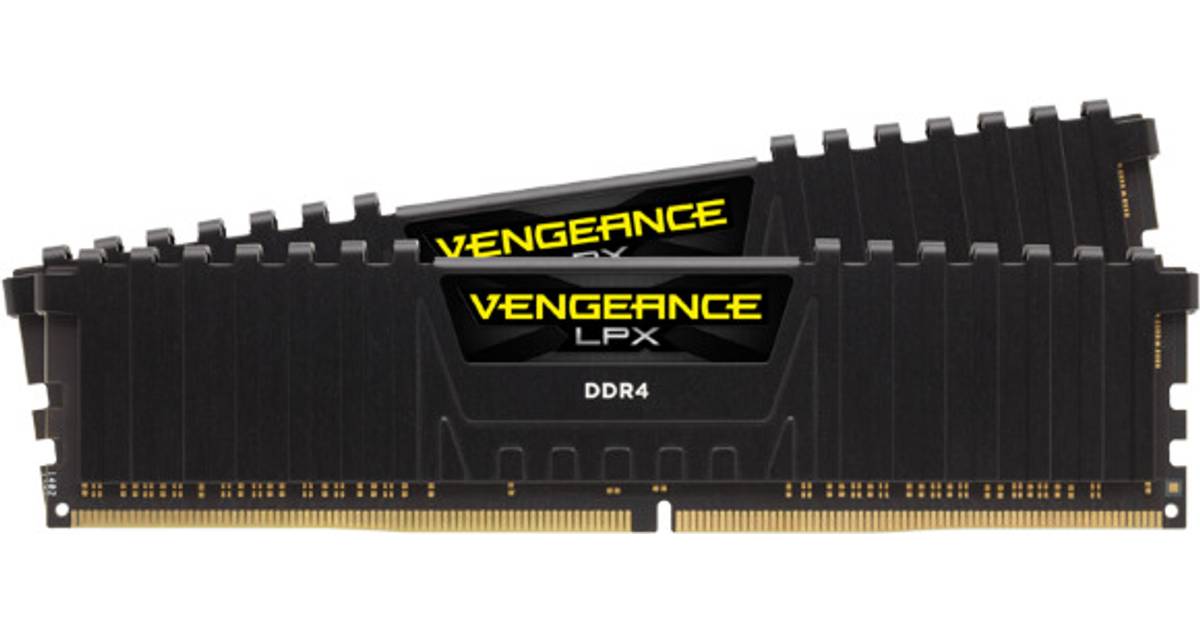
2x 8 GB Corsair Vengeance LPX (Hynix) CMK16GX4M2B3000C15 @ 2933 MHz
Fractal Design Edison 650 W

CPU-Z

I'm thinking with this board the best I could hope for is a 3200 MHz RAM speed and even that's depending on my luck with the sticks. What I'm hoping for is maybe a bit of a boost for FPS and a snappier desktop performance. I also read the CPU may be easier to OC with a lower voltage if the RAM timings are optimal, no idea if this is true.

The question is, is it worth it for the potential 200 MHz boost? I tried to trim the timings on the same memory back when I had a 1600X. Did the Thaiphoon & Ryzen DRAM Calculator thing by instructions, painstakingly inputting every figure in the BIOS only to not post and having to reset the CMOS. So I left it then because I had no idea why it didn't work nor how to continue. I'd also be much more inclined to overclock if it didn't involve repetitive CMOS resetting and removing the battery. Thankfully not every fail requires that. 😀

Thx for the input!
 
Last edited:
Solution
So I've read in several posts that the hassle of overclocking RAM might just be worth it. I've also been led to believe that there's relatively little returns in Overclocking the 3600. To begin with, here's what I've got:

Ryzen 5 3600 @ stock
ASUS Prime B350-Plus
2x 8 GB Corsair Vengeance LPX (Hynix) CMK16GX4M2B3000C15 @ 2933 MHz
Fractal Design Edison 650 W

CPU-Z

I'm thinking with this board the best I could hope for is a 3200 MHz RAM speed and even that's depending on my luck with the sticks. What I'm hoping for is maybe a bit of a boost for FPS and a snappier desktop performance. I also read the CPU may be easier to OC with a lower voltage if the RAM timings are optimal, no idea if this is true.

The question is, is it...
So I've read in several posts that the hassle of overclocking RAM might just be worth it. I've also been led to believe that there's relatively little returns in Overclocking the 3600. To begin with, here's what I've got:

Ryzen 5 3600 @ stock
ASUS Prime B350-Plus
2x 8 GB Corsair Vengeance LPX (Hynix) CMK16GX4M2B3000C15 @ 2933 MHz
Fractal Design Edison 650 W

CPU-Z

I'm thinking with this board the best I could hope for is a 3200 MHz RAM speed and even that's depending on my luck with the sticks. What I'm hoping for is maybe a bit of a boost for FPS and a snappier desktop performance. I also read the CPU may be easier to OC with a lower voltage if the RAM timings are optimal, no idea if this is true.

The question is, is it worth it for the potential 200 MHz boost? I tried to trim the timings on the same memory back when I had a 1600X. Did the Thaiphoon & Ryzen DRAM Calculator thing by instructions, painstakingly inputting every figure in the BIOS only to not post and having to reset the CMOS. So I left it then because I had no idea why it didn't work nor how to continue. I'd also be much more inclined to overclock if it didn't involve repetitive CMOS resetting and removing the battery. Thankfully not every fail requires that. 😀

Thx for the input!
Problem with 300 series chipset MBs is memory topology, only RAM with Samsung b-die chips was able to do any significant frequency boost above 2933MHz.
OC-ing to 3200MHz invariably gets higher memory latency negating much of a gain in total performance.
Instead of overclock see if you can get lower Cl. When I had a x370 MB I manage to lower Cl to Cl12 on my Kingston 3200 RAM, with Hynix M-die which gave me better overall performance than 3200MHz CL 15.
 
  • Like
Reactions: LrsLex
Solution
Instead of overclock see if you can get lower Cl. When I had a x370 MB I manage to lower Cl to Cl12 on my Kingston 3200 RAM, with Hynix M-die which gave me better overall performance than 3200MHz CL 15.

Okay... Any tips how to go about this? I've checked a couple of guides on tightening the timings and I frankly don't understand it at all. 😏
The Ryzen DRAM Calculator method tweaks just about every value in BIOS and I couldn't get that to work. Some guides talk about just changing a few values of those in the CPU-Z screenshot I posted. Like should I just input values according to this chart, leave the rest of it in BIOS as is and see how low I can go?

FrequencyCASRCDRPRASRCRRDSRRDLCCDLFAW
1067 MHz161515365046623
1067 MHz151515365046623
933 MHz141314314445520
933 MHz131314314445520
800 MHz121112273835517
800 MHz111112273835517
667 MHz10910223134414
667 MHz9910223134414

For example, could the values for 2133 MHz on the top line work for 2933? Like I said, I'm completely lost with this. 😆
 
Okay... Any tips how to go about this? I've checked a couple of guides on tightening the timings and I frankly don't understand it at all. 😏
The Ryzen DRAM Calculator method tweaks just about every value in BIOS and I couldn't get that to work. Some guides talk about just changing a few values of those in the CPU-Z screenshot I posted. Like should I just input values according to this chart, leave the rest of it in BIOS as is and see how low I can go?

FrequencyCASRCDRPRASRCRRDSRRDLCCDLFAW
1067 MHz161515365046623
1067 MHz151515365046623
933 MHz141314314445520
933 MHz131314314445520
800 MHz121112273835517
800 MHz111112273835517
667 MHz10910223134414
667 MHz9910223134414


For example, could the values for 2133 MHz on the top line work for 2933? Like I said, I'm completely lost with this. 😆
That is JEDEC table, need to look for XMP table. Thaiphoon burner http://www.softnology.biz/files.html can tell you more about your RAM and XMP profile of which highest should show about 1499MHz.
 
  • Like
Reactions: LrsLex
That is JEDEC table, need to look for XMP table. Thaiphoon burner http://www.softnology.biz/files.html can tell you more about your RAM and XMP profile of which highest should show about 1499MHz.

Here's the whole Thaiphoon Burner profile I exported to the DRAM Calculator:

Manufacturing Description
Module Manufacturer:Corsair
Module Part Number:CMK16GX4M2B3000C15
Module Series:Vengeance LPX
DRAM Manufacturer:Hynix
DRAM Components:H5AN8G8NAFR-TFC
DRAM Die Revision / Process Node:A / 21 nm
Module Manufacturing Date:Undefined
Module Manufacturing Location:Taiwan
Module Serial Number:00000000h
Module PCB Revision:00h
Physical & Logical Attributes
Fundamental Memory Class:DDR4 SDRAM
Module Speed Grade:DDR4-2133P downbin
Base Module Type:UDIMM (133,35 mm)
Module Capacity:8 GB
Reference Raw Card:A0 (8 layers)
JEDEC Raw Card Designer:SK hynix
Module Nominal Height:31 < H <= 32 mm
Module Thickness Maximum, Front:1 < T <= 2 mm
Module Thickness Maximum, Back:1 < T <= 2 mm
Number of DIMM Ranks:1
Address Mapping from Edge Connector to DRAM:Standard
DRAM Device Package:Standard Monolithic
DRAM Device Package Type:78-ball FBGA
DRAM Device Die Count:Single die
Signal Loading:Not specified
Number of Column Addresses:10 bits
Number of Row Addresses:16 bits
Number of Bank Addresses:2 bits (4 banks)
Bank Group Addressing:2 bits (4 groups)
DRAM Device Width:8 bits
Programmed DRAM Density:8 Gb
Calculated DRAM Density:8 Gb
Number of DRAM components:8
DRAM Page Size:1 KB
Primary Memory Bus Width:64 bits
Memory Bus Width Extension:0 bits
DRAM Post Package Repair:Not supported
Soft Post Package Repair:Not supported
DRAM Timing Parameters
Fine Timebase:0,001 ns
Medium Timebase:0,125 ns
CAS Latencies Supported:9T, 10T, 11T, 12T,
13T, 14T, 15T, 16T
Minimum Clock Cycle Time (tCK min):0,938 ns (1066,10 MHz)
Maximum Clock Cycle Time (tCK max):1,500 ns (666,67 MHz)
CAS# Latency Time (tAA min):13,500 ns
RAS# to CAS# Delay Time (tRCD min):13,500 ns
Row Precharge Delay Time (tRP min):14,061 ns
Active to Precharge Delay Time (tRAS min):33,000 ns
Act to Act/Refresh Delay Time (tRC min):46,500 ns
Normal Refresh Recovery Delay Time (tRFC1 min):350,000 ns
2x mode Refresh Recovery Delay Time (tRFC2 min):260,000 ns
4x mode Refresh Recovery Delay Time (tRFC4 min):160,000 ns
Short Row Active to Row Active Delay (tRRD_S min):3,701 ns
Long Row Active to Row Active Delay (tRRD_L min):5,300 ns
Long CAS to CAS Delay Time (tCCD_L min):5,356 ns
Four Active Windows Delay (tFAW min):21,000 ns
Maximum Active Window (tMAW):8192*tREFI
Maximum Activate Count (MAC):Unlimited MAC
DRAM VDD 1,20 V operable/endurant:Yes/Yes
Thermal Parameters
Module Thermal Sensor:Not Incorporated
SPD Protocol
SPD Revision:1.0
SPD Bytes Total:512
SPD Bytes Used:384
SPD Checksum (Bytes 00h-7Dh):51EDh (OK)
SPD Checksum (Bytes 80h-FDh):58B6h (OK)
Part number details
JEDEC DIMM Label:8GB 1Rx8 PC4-2133P-UA0-10

FrequencyCASRCDRPRASRCRRDSRRDLCCDLFAW
1067 MHz161515365046623
1067 MHz151515365046623
933 MHz141314314445520
933 MHz131314314445520
800 MHz121112273835517
800 MHz111112273835517
667 MHz10910223134414
667 MHz9910223134414
Intel Extreme Memory Profiles
XMP ParameterProfile 1Profile 2
Profiles Revision: 2.0
Profile 1 (Certified) Enables: Yes
Profile 2 (Extreme) Enables: No
Profile 1 Channel Config: 1 DIMM/channel
Speed Grade:DDR4-2998N/A
DRAM Clock Frequency:1499 MHzN/A
Module VDD Voltage Level:1,35 VN/A
Minimum DRAM Cycle Time (tCK):0,667 nsN/A
CAS Latencies Supported:20T,19T,18T,17T,
16T,15T,14T,13T,
12T,11T,10T,9T
N/A
CAS Latency Time (tAA):10,000 nsN/A
RAS# to CAS# Delay Time (tRCD):11,330 nsN/A
Row Precharge Delay Time (tRP):11,330 nsN/A
Active to Precharge Delay Time (tRAS):23,250 nsN/A
Active to Active/Refresh Delay Time (tRC):34,680 nsN/A
Four Activate Window Delay Time (tFAW):22,000 nsN/A
Short Activate to Activate Delay Time (tRRD_S):4,000 nsN/A
Long Activate to Activate Delay Time (tRRD_L):5,330 nsN/A
Normal Refresh Recovery Delay Time (tRFC1):350,000 nsN/A
2x mode Refresh Recovery Delay Time (tRFC2):260,000 nsN/A
4x mode Refresh Recovery Delay Time (tRFC4):160,000 nsN/A

And here's the calculator's values that I got:

Uofpr4H.png

So, Zen 2 since it's the 3600...
I set type to Hynix AFR, since AFR is in the component serial number:
H5AN8G8NAFR-TFC

Now, I left the DRAM PCB revision to manual as I don't know what my memory revision is. It says downbin in the Thaiphoon report, but I don't know if that means bad bin. Anyway, manual only lets you calculate the safe option. It says here that you can see which PCB the memory is, but it all looks the same to me without x-ray vision to see through the cover material. 🤔

index.php

Corsair-Vengeance-LPX-Black-DDR4-3000MHz-2x8GB-(CMK16GX4M2B3000C15).jpg


Guides to the calculator tell you to set the frequency to the RAM's namesake, so here to 3000 MHz, but importing the Thaiphoon data sets it to my current 2933. When I originally clocked the RAM to 3000 (from 2133, when the Ryzen 1 support got better) by the Asus DOCP, it automatically set it to 2933 and I just left it there since there really isn't any difference in performance. I guess it doesn't matter here either, except to put the right values in since some of them change between 3000 and 2933? Or maybe I should tweak the timings here at 2933 since it's proven to be stable at that speed?

How's that sound? Thanks!🤓
 
Tinkered around a bit but couldn't get anything manual to stick. Tried a couple of settings from the RDC, once even got to Windows but then BSOD'd. Minor progress though: the D.O.C.P Standard got the RAM speed from the 2933 up to 2994 MHz and even trimmed the timings a little from before.
qnYYAwW.jpg


edit.

Just remembered: my RAM sticks are in slots A1 and B1, when the MB manual recommends A2 and B2 slots. When I built the machine, it initially recognised only 8 gigs of RAM. Moved them to 1 slots and it worked. Might the slot selection affect OCing success?
 
Last edited: