ewancoder :
Pinhedd :
bwah? DDR4 is superior to DDR3 across the board.
You should really do some more research before you start spouting off such nonsense.
Not at all directions.
Sakkura :
DDR4 has a point-to-point topology, so it's beyond the limitations of dual channel, quad channel etc.
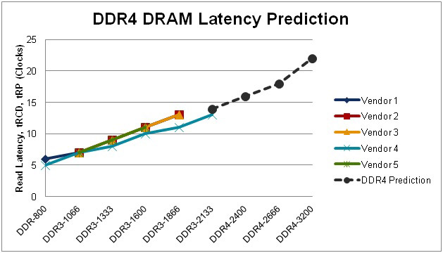
As for timings, bear in mind that DDR4 will have higher clocks which means the actual latency is lowered, if anything.
Well, i knew it. My point is that now ddr3 is capable of 2400-2600 Mhz on highest clocks, where ddr4 is still 2133 on lower clocks. It's just a matter of time when ddr4 becom 3+ GHz, but it's a matter of TIME. So it could be long time to wait, where ddr3 is NOW capable of 2400 plus lower timings.
*facepalm*
You seem to know just enough about DRAM to not realize that you do not know enough about it to make accurate statements.
The highest JEDEC standard DDR3 speed bin is DDR3-2133K (CAS 11), with DDR3-2133L (CAS 12) being the nominal standard. Many manufacturers produce modules with pin transfer rates much higher than this, or with timings tighter than that of the K bin, but these are all non-standard profiles. The highest JEDEC standard DDR2 speed bin is DDR2-1066E (CAS 6). Again, some manufacturers offer non-standard modules that use tighter timings or a higher IO bus reference clock.
On first inspection one might be tempted to claim that DDR2-1066E is faster than DDR3-2133L by virtue of having a lower CAS. However, SDRAM timings are measured relative to the IO bus reference clock itself. Double the transfer rate of the IO bus without doing anything to the module architecture itself and the latency doubles. However, the "real" latency (unlike that worthless chart that you posted) is measured in nanoseconds, not clock cycles. DDR2-1066E and DDR3-2133L both have real CAS latencies of 11.25 nanoseconds! DDR3-2133K is slightly faster at 10.3125 nanoseconds. One could just as easily take that chart and adjust the numbers for the DDR2 to DDR3 transition and it would look almost identical.
This of course discusses only timings, not other aspects of DDR4. Each generational leap in SDRAM has been accompanied by a doubling of the IO bus transfer rate relative to the module's internal operations. SDR SDRAM performed one transfer per module operation, DDR SDRAM performs two due to a 2n prefretch, DDR2 SDRAM performs 4 due to a 4n prefetch, and DDR3 SDRAM performs 8 due to an 8n prefetch. This has taken the DRAM interface from one that is fairly consistent (SDR SDRAM) to one that is very bursty (DDR3 SDRAM). The caveat here is that while the IO bus can easily deliver an instruction to a memory module, it then has to wait at least 11 nanoseconds before a response is generated, and that's only if the correct row is open. If the correct row is not open, the response will be much longer. So as the speed of the IO bus increases, it becomes increasingly idle as performance is bounded by the operation of the module itself.
To compensate for this, DRAM modules have multiple banks each with their own rows, and each able to have only one row open at a time. The memory controller can issue an operation to one bank, then switch to another and issue an operation to it, and then a third, and so on. Eventually it will swing back to the first bank to receive the results of the operation. SDR and DDR SDRAM have 4 banks each, DDR2 has 4 or 8, DDR3 has 8, and DDR4 has 16. An increase in the number of parallel banks is necessary to feed the faster IO bus. The 8 banks of DDR3 provide limited headroom for expansion, so reorganizing the module is necessary to feed the faster DDR4 IO bus.
It does all of this while drawing less power.


 RTX 4070 vs RX 7900 GRE faceoff: Which mainstream graphics card is better?
 Question New pc build r9 7900x3d rtx 4080 super no post only ram rgb turns on
 Question PC Shuts down during shader building on Last Of Us Part 1