News Intel Details Core Ultra ‘Meteor Lake’ Architecture, Launches December 14

Status
Not open for further replies.

TJ Hooker

Titan
Ambassador
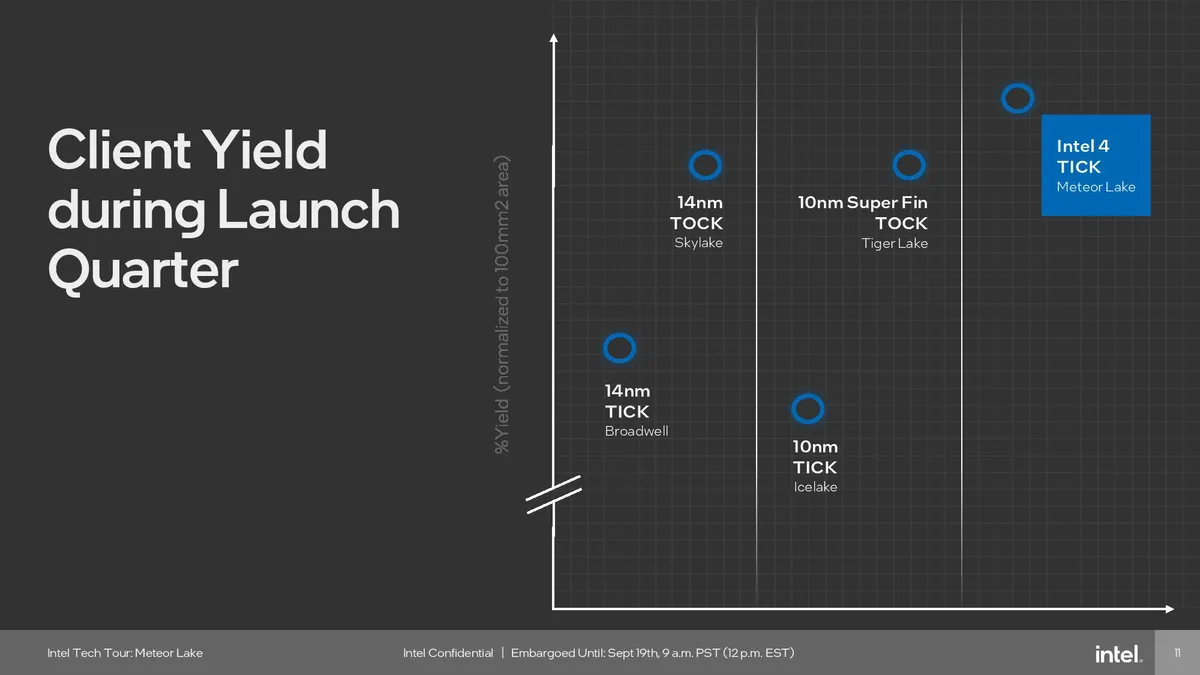
What do you mean?! I am sure they got 10nm to an extremely low loss of yield at some point because it was around for so long but this is about zero-day.
Zero day yields for 10 nm were presumably terrible, given the numerous delays and limited releases. 14 nm also had zero day yield issues, resulting in the delay/limited release of Broadwell. Those are the two nodes Intel has launched in the last decade.

Their point was that Intel's claim of having the best zero day yields in a decade (with Intel 4) doesn't say much, because that bar is set so low.
 
  • Like
Reactions: bit_user
Zero day yields for 10 nm were presumably terrible, given the numerous delays and limited releases. 14 nm also had zero day yield issues, resulting in the delay/limited release of Broadwell. Those are the two nodes Intel has launched in the last decade.

Their point was that Intel's claim of having the best zero day yields in a decade (with Intel 4) doesn't say much, because that bar is set so low.
oXFBXpwZpwdHPKHV7DyR4C-1200-80.jpg.webp
It has a better initial yield than the refinements of the two previous nodes.
That's still impressive.
 
Sep 19, 2023
2
1
10
oXFBXpwZpwdHPKHV7DyR4C-1200-80.jpg.webp
It has a better initial yield than the refinements of the two previous nodes.
That's still impressive.
Quite surprised to see this interpretation. It seems fairly clear to me that it's comparing zero day to zero day, not zero day to refinements. Am I just blind? ;P TJ Hooker has it correct, as far as I can tell.
 

spongiemaster

Admirable
Dec 12, 2019
2,280
1,285
7,560
Zero day yields for 10 nm were presumably terrible, given the numerous delays and limited releases. 14 nm also had zero day yield issues, resulting in the delay/limited release of Broadwell. Those are the two nodes Intel has launched in the last decade.

Their point was that Intel's claim of having the best zero day yields in a decade (with Intel 4) doesn't say much, because that bar is set so low.
It may not be impressive, but it is important. Intel needs to start consistently delivering on its roadmap. With Intel 4 reaching market this year, it's only a few months late vs their roadmap from 2021, which had Intel 4 products on the market in H1 of 2023. That's world's better than 10nm, and also better than 14nm.

As Terry pointed out, it's also comparing vs the refinements of 14nm and 10nm, so this really is a noteworthy achievement.
 

TJ Hooker

Titan
Ambassador
oXFBXpwZpwdHPKHV7DyR4C-1200-80.jpg.webp
It has a better initial yield than the refinements of the two previous nodes.
That's still impressive.
Ah, I missed that slide. I was just going off the article text, which I interpreted as comparing zero day to zero day yields. Yeah, if Intel 4 yields are already better than mature 14nm and 10nm SF, that is much more impressive.

Edit: Well, maybe not "mature", as Skylake was fairly early in the lifespan of 14nm (and potentially a similar story with Tiger Lake, if you consider 10nm ESF/Intel 7 to be a maturation of 10nm SF). But not "zero day".
 
Last edited:
  • Like
Reactions: bit_user

JamesJones44

Reputable
Jan 22, 2021
710
662
5,760
When I read the headline about 2x performance on the iGPU I assumed it would be with the memory on chip vis over chip I/O to the MB.

Looks decent overall, but will have to wait for the benchmarks to get a sense of how much progress Intel has actually made.
 

jasonf2

Distinguished
I think the point he was trying to make is that the 4 process node is on track and not going to be another 10nm no show. Refinements or not 10 nm never really made it out of the gate hence 14nm+++++++++++.
 
Sep 19, 2023
2
1
10
Ah, I missed that slide. I was just going off the article text, which I interpreted as comparing zero day to zero day yields. Yeah, if Intel 4 yields are already better than mature 14nm and 10nm SF, that is much more impressive.

Edit: Well, maybe not "mature", as Skylake was fairly early in the lifespan of 14nm (and potentially a similar story with Tiger Lake, if you consider 10nm ESF/Intel 7 to be a maturation of 10nm SF). But not "zero day".
Thanks very much for explaining this further. I missed that too. Apologies, also, TerryLaze.

 
  • Like
Reactions: bit_user

everettfsargent

Honorable
Oct 13, 2017
130
35
10,610
That chart has no labeled y-axis units! Anyone else notice break on y-axis? Bueller ... Bueller ... Bueller ...

So 10% yields go to 11% go to 12% meaning improvement but insignificant improvement, n00bs!
 
  • Like
Reactions: bit_user

bit_user

Polypheme
Ambassador
I hadn't previously thought about it in these terms, but the story of computing, for pretty much my whole life, has been one of increasing integration. The SoC is like the holy grail of that, where all the key elements of an entire system (aside from memory and storage) are packed onto a single chip/die.

With Intel now going all-in on chiplets/tiles, it's a slight reversal of that trend. Intriguing.

KU3PiA5EbUeaZAiBz4QdQh.jpg

 
  • Like
Reactions: Order 66

bit_user

Polypheme
Ambassador
I think the point he was trying to make is that the 4 process node is on track and not going to be another 10nm no show. Refinements or not 10 nm never really made it out of the gate hence 14nm+++++++++++.
Intel's 10nm shipped, eventually!

Cannon Lake was the only commercial product made on their original 10 nm node, and it was so bad they basically buried it.

The improved 10 nm node was used for Ice Lake quad-core laptop & (up to 38-core) server CPUs, as well as Jasper Lake and Elkhart Lake (quad E-core SoCs).

Next came the 10 nm SuperFin node, used for Tiger Lake - another laptop SoC, but this time they even had an 8-core version.

Finally, 10 nm Enhanced SuperFin (rebranded as Intel 7) was used for Alder Lake. A further-refined version was used for Raptor Lake.

So, it effectively took 10 nm+++, before the node was finally ready to supersede their 14 nm series, on the desktop.

Moving on to Intel 4, it's not all good news. Let's not forget the small detail of how Meteor Lake was cancelled from the desktop, echoing what happened with Ice Lake and Tiger Lake. That clearly wasn't planned, or else you'd think they'd have a better fallback plan than Raptor Lake "Refresh". However, I think it happened so late, there simply wasn't time to do any proper revisions of the sort they did in Gen 13.
 
  • Like
Reactions: Order 66

jasonf2

Distinguished
I hadn't previously thought about it in these terms, but the story of computing, for pretty much my whole life, has been one of increasing integration. The SoC is like the holy grail of that, where all the key elements of an entire system (aside from memory and storage) are packed onto a single chip/die.

With Intel now going all-in on chiplets/tiles, it's a slight reversal of that trend. Intriguing.
KU3PiA5EbUeaZAiBz4QdQh.jpg
I may be a little off base here but I don't really see tiles on top of an interconnect fabric being a reversal of that trend at all. A monolithic die SOC has been facing scaling issues for some time now. There are simply a number of very important integrated functions that not only get no gains from going smaller but may actually suffer for it, or at the very least get little to no gains for the expense of reinventing the wheel every time a new node comes out. Tiles allow reuse scenarios that will further increase integration. We are moving into an era where simply shrinking the node isn't going to increase performance. The big gains to be had are going to be task specialized cores, massive parallelism, software reprogrammable cores and AI driven predictive scheduling / core task routing. Shrinking the die without the ability to differentiate nodes on the same package simply means that more has to move off of package. In theory tiles could actually allow SOC memory and storage to move onto the package whereas monolithic die packages were simply too inflexible to do that.
 
  • Like
Reactions: Order 66

bit_user

Polypheme
Ambassador
I may be a little off base here but I don't really see tiles on top of an interconnect fabric being a reversal of that trend at all.
You have to squint, a little bit. However, we've had mass market multi-chip packages going back at least as far as the Pentium Pro (1995), and the direction of travel was clearly towards monolithic dies.

Even concerning multi-core CPU, some of the first examples we saw merely packed multiple dies in the same package (Pentium D), later followed by integrating them on the same die.

Next to get integrated into a monolithic die were GPUs. Intel and AMD first had GPUs integrated into their motherboard chipset. Then, in the first gen of "Core"-branded CPU, Intel moved the GPU die into the CPU package, but they were still separate dies. Sandybridge was Intel's first gen that had them integrated together, in a monolithic die.

Starting with the FPU, then the Northbridge, block after block got directly integrated into monolithic dies, sometimes with a half-way point as a discrete die in the CPU package. As far as trends go, you really can't miss it.

A monolithic die SOC has been facing scaling issues for some time now.
Don't get me wrong. I'm not arguing against chiplets or tiles. I know all the rationale behind this new shift. I just wanted to point out what a marked departure it signifies.

or at the very least get little to no gains for the expense of reinventing the wheel every time a new node comes out. Tiles allow reuse scenarios that will further increase integration.
Heh, one interesting downside Intel is facing is having to restrict the new instructions in their Arrow Lake P-cores and E-cores, because they decided to reuse the Meteor Lake SoC tile, which contains those Crestmont E-cores. Therefore, the other cores had to be held back to maintain ISA symmetry.

We are moving into an era where simply shrinking the node isn't going to increase performance.
Let's not get ahead of ourselves. Yes, SRAM scaling is an issue, and before that was I/O scaling. However, logic density and perf/efficiency are still improving with newer nodes.

The big gains to be had are going to be task specialized cores,
Beyond AI and graphics, I'm skeptical about this.

AI driven predictive scheduling / core task routing.
That's largely orthogonal to the other stuff we're talking about.

In theory tiles could actually allow SOC memory and storage to move onto the package whereas monolithic die packages were simply too inflexible to do that.
I think you're confused. The whole discussion of monolithic vs. chiplets has nothing to do with on-package memory.

Apple still uses monolithic dies (except for M-series Ultra) and they have on-package memory. GPUs largely remain monolithic, and have used on-package HBM since 8 years ago. Around that time, Intel's Xeon Phi was also monolithic and incorporated 16 GB of MCDRAM.

As for storage, it's much less heat-tolerant (and more failure-prone) than DRAM or logic. So, it really doesn't make sense to bring it on-package (leaving aside some specialized embedded products).
 
I think you're confused. The whole discussion of monolithic vs. chiplets has nothing to do with on-package memory.
It's called system on chip, and not system on monolithic die...
Chip includes everything contained in the CPU.
There is no "whole discussion of monolithic vs. chiplets" , you are the only one that brought it up, for no good reason, Integrating the ram and storage is the next logical step, correction, it's not the next step since it's already done.
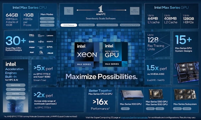
Intel's CPU max has the ram integrated and you can use it as main storage.
Intel_Max_Series_product_information.jpg
 
  • Like
Reactions: Order 66

bit_user

Polypheme
Ambassador
It's called system on chip, and not system on monolithic die...
Chip includes everything contained in the CPU.
"chip" is short for microchip, which is literally a die. Although, some people informally use the word "chip" in a more inclusive fashion.

You can see examples of this, in the way that multi-die products were originally called "MCMs" - Multi-Chip-Modules.

There is no "whole discussion of monolithic vs. chiplets" , you are the only one that brought it up,
Of course there's a discussion of monolithic vs. chiplets. I mentioned it in reference to the article content, which I cited, and @jasonf2 responded. That makes it a discussion.

for no good reason,
I was pointing out that there's a significant trend-reversal, here. I didn't expect anyone to take issue with that observation, but I gather @jasonf2 misunderstood my post as a critique or somehow arguing against chiplets/tiles, which I wasn't.

Integrating the ram and storage is the next logical step, correction, it's not the next step since it's already done.
I already cited several examples of on-package memory. No, it's not new. You seem to have overlooked the fact that I even credited Intel for it, in Xeon Phi.

Intel's CPU max has the ram integrated and you can use it as main storage.
I'd ask you for clarification, except I know you're flat-out wrong on this point. Storage = persistent media, like NAND flash. No, making a ramdisk doesn't somehow magically transform RAM into storage. It's still just RAM, because it forgets everything once you lose power.
 
"chip" is short for microchip, which is literally a die. Although, some people informally use the word "chip" in a more inclusive fashion.

You can see examples of this, in the way that multi-die products were originally called "MCMs" - Multi-Chip-Modules.
Then were do you see the regression, did intel also already do a previous soc tile/die that had more stuff on it?!
You either see the whole CPU as a whole CPU or each tile/chiplet as its own chip, in either case the new ones have the same amount or even more stuff on them.
I'd ask you for clarification, except I know you're flat-out wrong on this point. Storage = persistent media, like NAND flash. No, making a ramdisk doesn't somehow magically transform RAM into storage. It's still just RAM, because it forgets everything once you lose power.
Fine. But it would not provide any kind of challenge to add persistent media to that thing, heck they could substitute part of the ram with optane.
 
  • Like
Reactions: Order 66

bit_user

Polypheme
Ambassador
Then were do you see the regression, did intel also already do a previous soc tile/die that had more stuff on it?!
Well, this is a high-volume, mainstream product. I'm well aware of Lakefield and Ponte Vecchio. Both technically, very impressive and a sign of things to come, but only now are we seeing these developments reach most consumers.

But it would not provide any kind of challenge to add persistent media to that thing, heck they could substitute part of the ram with optane.
I think there are two big challenges in trying to integrate storage on-package: space and temperature.

NAND chips already make extensive use of 3D stacking, and you can see with your own eyes how many it takes to achieve decent capacities by simply looking at everything on a M.2 drive other than the controller. Now, imagine all those chips crammed next to the CPU die! You'd pretty quickly run out of room before achieving much capacity.

Furthermore, as I've mentioned, NAND doesn't like high temperatures. It looses charge faster, requiring more frequent cell rewrites, and that ultimately results in accelerated wear. Regarding Optane, the specs I can find seem to indicate a broader temperature range, but CPUs run pretty hot these days and even having a limit of 85 C might be an issue:

Getting back to the first point, Optane is less dense than NAND. So, again, you'd have trouble equipping very much in the space available.

Finally, there's the issue of performance. During typical machine operation RAM is accessed thousands of times more heavily than storage. The native performance of DRAM is also higher. Both of these are reasons why you want RAM to have a high-bandwidth connection to the CPU and why doing so is more practical than storage. Even the latest, greatest Optane PMem module I linked above has bandwidth an order of magnitude less than DRAM. According to this, it's just 3 GB/s (random) to 6 GB/s (sequential):

So, all practical issues aside, the benefit of squeezing storage on the same package as the CPU die is highly questionable. Add to that, the fact that you couldn't replace faulty storage or increase capacity without replacing your CPU, and it really looks like a very undesirable solution.
 
Status
Not open for further replies.