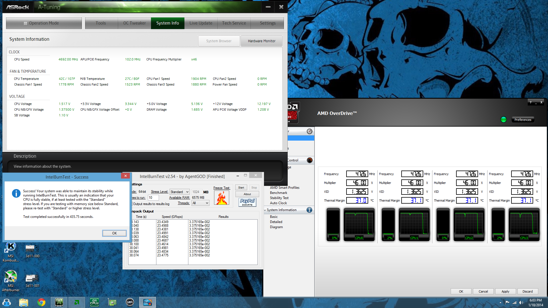
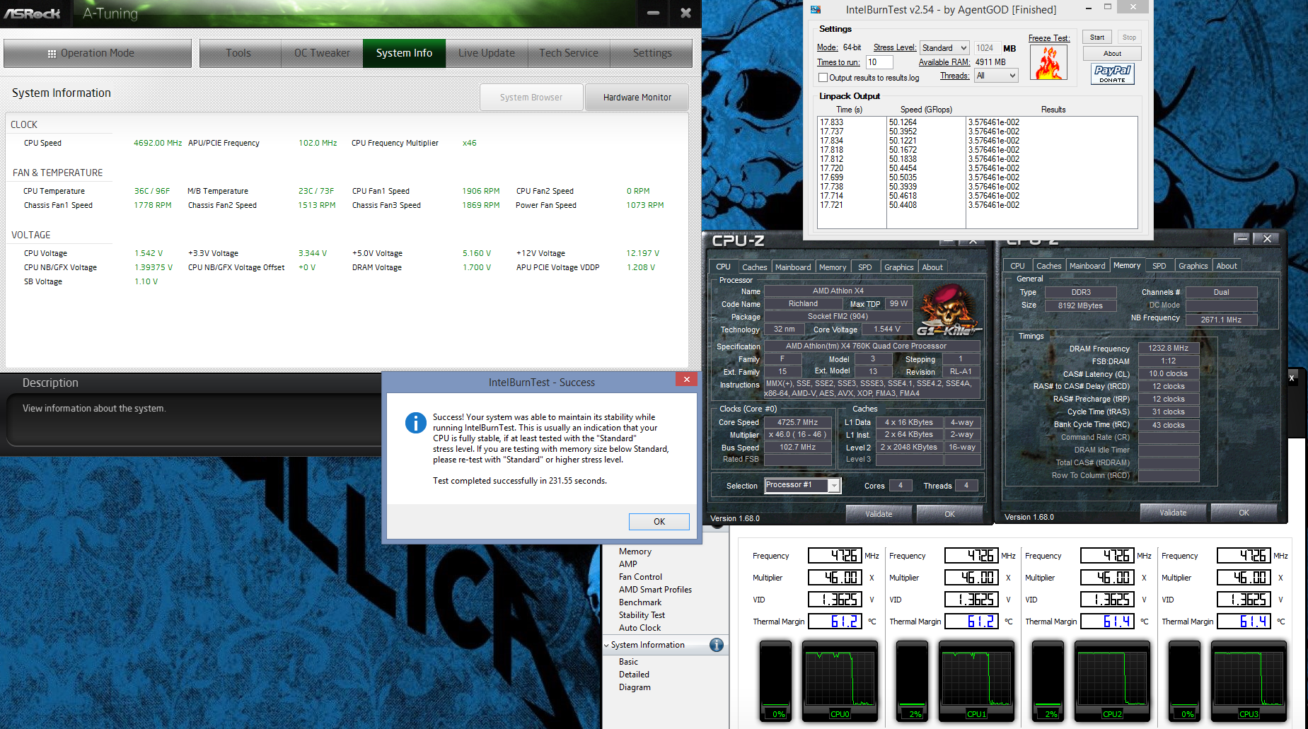
ta152h :
anyone else notice that Kaveri was within 5% of the ipc of sandy bridge at similar clock speeds...
how did we miss this when Kaveri came out?
Because people were smart enough to know what you're saying isn't true.
An i3 has two real cores, so if you want to compare a real Sandy Bridge with a Steamroller (which shares the FPU, but otherwise the cores are 'real'), you'd compare with an i5. Steamroller gets molested, and left to runt off seeking professional help and counseling.
These are very badly designed processors. They have huge GPUs, but not enough memory bandwidth to feed them.
By the way, other sites did test the A8-7600 against the A10-7800, with the latter having better performance in the vast majority of benchmarks. Not by a lot though, in most cases.
But, in one sense the A8-7600 is a more balanced design, since the GPU is smaller and better matches the inferior memory controller on the chip. The bad part is, this is just a castrated part, so the die is still huge and part of it is disabled. AMD would have been better off just making this die, and forgetting about the bigger ones, since they're so bandwidth limited. Doing so would have made the chips significantly less expensive to make.
If they don't improve the lousy memory controller, throwing more transistors into the GPU isn't going to yield the types of results they are looking for. Obviously, the new memory they are looking at will help, but they should also make an effort to improve the terribly inefficient memory controller so it gets somewhere in the neighborhood of where Intel is. Even in the same county. Or state. They're not even in the same planet, which makes you wonder why they don't look at Intel's design more closely. Even several generations units use memory better than AMD's, so they've had time to copy it, or to get ideas how to use it in their crippled chips.
smart enough? how about you read the article a little closer before you start to toss about insults.
you obviously didn't read the article. in the ONLY single threaded test run, the kaveri was 95% the power of the sandybridge, controlled for the same clock speed. It takes a little math to work out (since they were benched at different speeds) but it works out to the kaveri being just off the pace of a Sandybridge. Of course once he got into the generic synthetics that single core parody vanished which raises questions to his home made benches.
I know I've seen the benches in the past, with kaveri basically being on par with a phenomII in IPC... and a solid 15%-20% slower in single core performance then a sandybridge... so i was a little surprised that the lone -non-synthetic test resulted in such a small performance gap. that's all i was pointing out.
As an aside, these are not poorly designed chips... these are actually rather complex and fairly well designed all things considered. The issue at play is the focus of the design of bulldozer is both inspired and inherently flawed. Bulldozer was designs on a "modular" archetecture, the idea was with the bulldozer design they could custom make cpus to fit specific clients needs cheaper. It worked so well they landed the 2 next gen console, because frankly... it was cheaper and easier for them to individually design a cpu for them then anyone else due to the modular design of bulldozer.
The problem is with modular and flexible design comes trade offs. one of them is they simply can't compete with intel's performance tuned product line... furthermore bulldozer ended up with some crippling internal design faults that prevented it to SCALE up as well as it scaled down in short at lower voltages and lower clocks it's ipc actually is higher then it is at higher voltages and higher clocks... the result it its far more competitive on the low end with intel then it is on the high)
Finally anyone who talks about a bulldozer cored cpu as having "fake" cores needs to check their inter intel fanboy at the door
The engineering definition of a cpu "core" is that a core must have 3 parts
1) instruction control unit
2) instruction execution unit
3) input/ouput unit
AMD's bulldozer family cpu cores have all of these parts; each core module contains 2 separate cores, each one of those cores has their their own scheduler (control unit), 4 execution units, and an I/O unit.
The confusion about the bulldozer architecture, comes from the floating point processor unit. You see up until 2000 or so, no cpu had a floating point processor. In fact computers around 1997 started to include math-coprocessors add on boards to handle the floating point math... around 2000 cpus started to integrate the math coprocessor, called a floating point processor onto the cpu itself. These units basically handle floating point math (calculus) which traditional cpus rather suck at. Now understand, these floating point processors are completely separate units from the cpu core on both an AMD and Intel cpu... in a way they're sorta the progenitor to the whole concept of an APU, as all a gpu really is, is a highly specialized math coprocessor or calculus calculator. AMD chose, with bulldozer, to place 1 256-bit floating point processors on their cpu per core module... that single FPU is naturally a 256-bit unit, but when needed can function like 2 128 bit FPUs, THIS is the part that works like a gimped version of intel's hyperthreading; as in it's a single FPU which can at times, when needed handle 2 instructions at the same time.
The fx cpus ARE by every definition proper 4/6/8 core cpus. They just work a little different with their design then an intel cpu... or even the older retired AMD k10 architecture
**as a disclaimer i quoted the bit at the end from one of my own forum posts in another web forum (overclock.net) posted under the username azanimefan, this was not stolen from another poster, i just didn't feel like typing that all out again**

 ).
).

