AMD CPU speculation... and expert conjecture

Page 709 - Seeking answers? Join the Tom's Hardware community: where nearly two million members share solutions and discuss the latest tech.
Status
Not open for further replies.

juanrga

Distinguished
BANNED
Mar 19, 2013
5,278
0
17,790


No. I am claiming something completely different. Read my last resume post on ARM to get the point, because you didn't get it still.


I am not assuming that. It seems you missed when I said that Nvidia optimized the GPU for graphics, whereas AMD is pushing a nonsensical compute approach that hurts the cards on graphic tasks.


AMD is developing the compute part of GCN for APUs and then reusing the same graphics architecture on dGPUs for reducing costs. AMD is not developing any "GPGPU beast"; in fact AMD's chances of conquering the GPGPU market are zero.


And again you mix efficiency with power consumption, whereas fail to understand why Nvidia, IBM, Intel, and everyone else takes efficiency as first priority those days. Sorry, I am not going to explain the same once more: 10 times is enough!
 

juanrga

Distinguished
BANNED
Mar 19, 2013
5,278
0
17,790


Another prediction from gamerk confirmed. The dual-core Intel scales up under DX12 and performs so well as quad-cores AMD.

The gap between Intel and AMD is reduced under DX12 on the extreme quality set, because the 770 is the bottleneck. I think that if AT had used a 980/290X instead, the i3 would perform significantly ahead of AMD quad-cores, as in the low quality set.
 

bmacsys

Honorable
BANNED


There is no L3 because there is no room on the die.
 

bmacsys

Honorable
BANNED


You think you know more than the technical staff at AnandTech now? Kind of like how you told Linus Torvalds that he doesn't know what he is talking about. That "debate" you had with Linus was pure comedy gold.


That is the consequence, not the reason.

They have no L3, because they decided to design the APU without it. We just speculated why and how.

Cheers!
 

juanrga

Distinguished
BANNED
Mar 19, 2013
5,278
0
17,790


You got it backwards. The die is small because there is no L3.
 

truegenius

Distinguished
BANNED


z1HFhze.jpg

also
JD2B9Lq.jpg


there is no l3 because apu is for budget segment and thus need to remain small in die size thus "no room for l3" stand correct
and because they didn't included die consuming l3 as a result "die is small" stand corrected
looks like you like to dig mistakes in people's comments
and i like to dig meme for your replys :whistle:
 

blackkstar

Honorable
Sep 30, 2012
468
0
10,780


Please tell me you have a link. PM me if you have to. People who think they know Linux and actually don't are so entertaining.

Anyone heard of HM1 socket? Maybe FX8350 wants to drop some subtle hints for us if it may exist or if it's someones random fantasy?
 

Cazalan

Distinguished
Sep 4, 2011
2,672
0
20,810


Part of it its in my sig.

As for HM1 it comes from a new Seronx post. http://semiaccurate.com/forums/showpost.php?p=229524&postcount=1095

I saw it there first anyway. As for validity, well, he digs up some weird stuff at times.
 

Cazalan

Distinguished
Sep 4, 2011
2,672
0
20,810


Good article really. They did get some efficiency gain on the A57 core but the A53 core lost efficiency. Of course if you want more compute power you get the familiar ramps as the f*V^2 rises. And there is a sharper rise at the 1.6Ghz mark essentially showing where the overclocking begins.

The big.LITTLE continues to be a mixed bag. Too complex to schedule even after 2 years in use.

And yes the legacy code problem is hitting them too. Lollipop ramp is going WAY slower than any of the previous releases. People think it's just a matter of recompiling but its not.

Of course these are cell phones so as long as surfing is faster they'll be happy right? ;)
 
Gone for a few days and some bad juju gets put out.

L3 cache most certainly does not give anywhere near 40% performance increase, you'd be lucky to see 15% at best.

"Cache" just serves as a temporary holding ground for data that isn't yet needed, therefor it runs into rapidly diminishing returns. The most important cache in your CPU is the 32kb of L1 I/D cache, it would double if not triple the performance vs not having it. Adding another 32kb of L1 I/D would not cause another doubling / tripling. The same thing happens with L2, 32kb of L2 would be nearly inconsequential, you'd need 128KB or more to see an impact. L3 has even worse scaling, you need many megabytes worth to see any impact. L4 would be horrible performance vs quantity, you'd need 64~128MB worth for it to be worthwhile.

This is because CPU's can only operate on data in registers and registers are very small holding only a few bytes worth of data. It's the job of the instruction scheduler to ensure those bytes of data are stored in the L1 Instruction / Data caches so that they can be copied into the registers when the load / store instruction is called. If it's not in the L1 cache then it must go looking into the L2 cache, which is much slower then the L1. If it's not in the L2 then it has to go to the L3 which is itself much slower then the L2. And if it's not in the L3 then it's off to main memory while your performance stalls out. Because L3 is so much slower then L2 and ridiculously slower then L1, it has a much more marginal impact on performance then the previous two. Cache is made from SRAM which takes up a sh!t ton of die space and power, out of all the components on a CPU it's the L3 that has the worst cost vs space vs heat vs performance.

Look at how much space that 8MB L3 cache memory takes up, its nearly half the size of the CPU.
http://images.bit-tech.net/content_images/2012/11/amd-fx-8350-review/piledriver-3b.jpg

Now look at much space the iGPU component of the Trinity APU takes up.

http://images.anandtech.com/doci/5831/LabelledDie.png

If your going to bolt on a powerful iGPU you need to remove something otherwise your going to get a hugely expensive chip. That something is the L3.

This is what a Phenom II looks like, again notice the size of the L3 cache

http://www.examiner.com/images/blog/replicate/EXID46735/images/phenom_ii_x6%282%29.jpg

And now to crush all the BS going about about the Phenom II. The 32nm version known as Llano (K10.5) actually had double L2 cache then the 45NM version. Doubling the L2 will give a larger performance increase then adding L3 due to lower latency of the L2. Phenom II had 64KB L1 I/D 512KB of L2 and 4~6MB of shared L3. Llano had 64KB of L1 I/D and 1MB of L2 with the L3 removed and an iGPU bolted on. Since the L2 was already fairly large adding slow L3 wouldn't of been much of a performance if any. AMD also use's a victim cache system whereby data is not duplicated across the different cache levels, Intel doesn't and the contents of the L1 are also stored in the L2 which is all stored in the L3, so exact size's are not comparable between them. Intel's design actually has less usable cache then AMD's but since their predictor is so much better, they have fewer miss's.

Which brings me to why you see lower IPC in the BD uArch vs K10 and SB. AMD's predictor technology is significantly behind Intel's, they produce cache miss's more often. What really hurt BD was the longer latency in the L2 cache (and nearly unusable L3), when those miss's occurred you need to stop everything and wait those clock ticks for the right data to be retrieved. As the BD uArch was designed to be clocked much higher then the K10, they implemented larger buffers and higher latency (in a simliliar way that DDR4 has higher latency then DDR3 which has higher then DDR2). Whenever your forcibly downclock a BD/PD/SR uArch CPU, your deliberately crippling it by not lower it's latency. This is why I laugh at the stupidity of comparing two different uArch's at the same clock speed. Only absolute performance for absolute cost matters, no matter how the engineers decided to get there.
 
I'm gonna do this part as a second post because it's kind of complicated.

You can't put more then one signal down a single pathway inside an integrated circuit (IC), if you try then you can get unpredictable and random results. CPU's are extremely complicated things made up of tens of thousands of individual circuits and functions. In order to prevent having two signals put down the same pathway there are deliberate wait states engineered into every connection. Those wait states are expressed as clock ticks. The time it takes an electron to get from point A to point B is highly dependent on the conditions of the circuit and path it's taking, but that time is measured in real time units like picoseconds or nanoseconds. Those two different concepts need to be worked out together, the time it physically takes for a packet of electrons to get down a path and the time the circuit should wait until sending another packet. Engineers design in static wait timers based on a target speed for the entire uArch, those timers are measured in clock ticks. Since some silicon is better then others, some chips will be able to physically send those packets faster then other chips and thus some chips will have more stability at higher clock speeds vs other chips. Since the wait states are not variable, clocking a chip under it's rates speed imposes longer timers on how often a circuit can send data.

An example would be a circuit that could send a packet of data every 5ns, the engineers then impose a 5 tick wait state which cause's the circuit to wait 5 clock ticks before attempting to send another packet. If you were to raise the clock speed then you'd be sending data faster then every 5ns, possibly every 4ns, if the circuit couldn't physically handle it then it would crash or you'd have to send the data faster (higher voltage means faster electrons at the expense of higher KE when the electrons strike something). If you were to lower the clock speed then you'd be sending data less frequently, down to once every 7ns, half the clock speed would be sending it every 10ns.

It should become obvious why trying to compare different design's at the same clock speed is stupid, they each have different wait states hardwired based on the projected clock speeds. Chip uArch A maybe clocked at 3ghz with a 5ns wait time, Chip uArch B may clock at 4ghz with the same 5ns wait time. Clocking chip uArch B down to 3ghz would raise that delay to 6.6ns even though the silicon is perfectly capable and engineered for 5ns.

That should also explain why and how binning works.

#Note#

This is a very simplified version of this, classic electronics theory is an entire area of study into itself, not to mention how quantum mechanics interprets things differently. In classic theory free electrons don't actually move much but instead transfer their energy from one molecule to another down a path with a set velocity. Whats changing is the molecules inside the semi-conductor. I strongly encourage anyone interested in this to do their own research, it'll be many nights of reading and rereading but it'll be worth it in the end.
 

noob2222

Distinguished
Nov 19, 2007
2,722
0
20,860
CPU_001.png


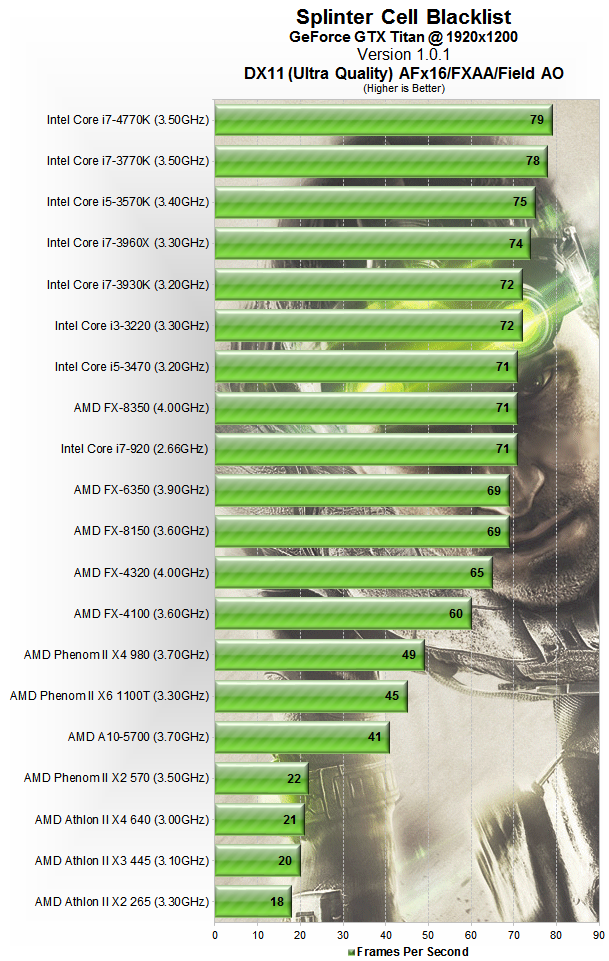
I didnt say 40% any time, but can be as much as 40%, granted this one is 32% with 100 mhz higher clock on the a10 5700 vs 4100-fx, both piledriver cores.

Either way, its a significant hit not having l3 cache, well over 15%.
 

what if the api i.e. directx had something to do with the performance difference?


HT is just offering a second set of external x86 registers to the OS for scheduling. There are four ALU's inside Haswell vs three in SB/IB, that is where the extra performance is coming from. The wait states I was talking about are static, it's literally how many clock ticks until the gate signals it's available for another signal. There are thousands of these connections all over the CPU and they play a very large role in determining how many cycles it takes to do any particular function. The shorter the distance the less time it takes for the electrons to down that path. Raising the clock rate doesn't increase the speed of the electrons (unless your also raise voltage) so you will eventually get to a point where your trying to push another set of electrons down the path before the first set has arrives, that is where you get instability. Raising the clock rate will reduce the period of time in-between bursts of electrons. HT is a high level function compared to signal latency, it's not really connected.

Either way, its a significant hit not having l3 cache, well over 15%.

And no, L3 doesn't give you more then 10~15% period. It's not some magic cure that suddenly increase's performance. It only ever gets used when your predictor scores a miss on L1 Instruction / Data and also scores a miss on L2 victim cache. That rarely ever happens, we are talking single digit percentages or less because if it happened anymore you'd get extreme stutter and unpredictable results.

I swear sometimes when I'm trying to explain this stuff I feel like this
 

blackkstar

Honorable
Sep 30, 2012
468
0
10,780


Hyperthreading has always been improving each generation. With Nehalem, most people turned it off because it would hurt performance more often than help. When I had my Nehalem, I turned HT off when I was gaming and left it on when I was doing multi-threaded work. Apparently after looking over various forum posts, that's not the case anymore.

I keep seeing people jump at AMD using SMT and thinking it'll be just as good as Intel's SMT. It won't be. SMT is not something easy to do and it's easy to screw up. Intel's first CPUs with hyperthreading came out in what, 2003? And it took them until SB, IB, or arguably Haswell to actually get it right.

As palladin said, SMT is only really helpful if the rest of your architecture can take advantage of it. And the parts that SMT wants in order to perform well are the ones that AMD struggles with the most.

Look at how AMD responded to SMT on Intel parts. They released real dual cores. I'm guessing CMT was AMD's answer to SMT on x86 being sort of a joke that most consumers to this day don't actually want or need, but it didn't pan out right for various reasons that have been beaten to death.

AMD going back to SMT feels like they'd be taking a step backward and trying to just compete with Intel directly. AMD does best when they are doing unique things that Intel isn't doing. The problem is that's high risk, high reward style development. With something like K8 and moving IMC to CPU, it was a huge win. With something like CMT, it wasn't so much. AMD trying to make an Intel-style core with their funds, compared to Intel's, would be an absolute blood bath for AMD.

And I realize a lot of you are probably thinking "well AMD will just fix these problems in Zen!" It's not so easy. The path to a good branch predictor is very difficult. It's not an easy thing to do, you're basically asking a bunch of transistors to predict the future. And to top it off, the road to a good branch predictor is laden with patents that you have to avoid. The last thing you want to do is design a CPU, have some patent troll show up and go "that's our patent, give us x% of your profits or we're going to sue you non-stop!"

You should know how messed up the patent system is for software and hardware. I've heard people come out and basically say that the situation is sort of like there's really obvious, simple ways to do things that make the most sense, but they're patented so if you don't have the patent, you have to license or do something else.


Ok fair enough, however in that case why is Trinity performing so much slower than the FX4100 in that benchmark then? Both are 'quad core' parts in AMD parlance, and actually the 4100 in a generation older. With the exception of L3 cache, I really can't see what benefit the FX has over the A10 (in fact theoretically the FM2 platform is more modern than AM3+ including PCIe3.0 which should provide a slight benefit to the Titan). There's something strange going on there...
 

noob2222

Distinguished
Nov 19, 2007
2,722
0
20,860
Paladin, please explain then why certain games suffer 30% or more with the lack of l3 cache?

I gave one example, and was told "it doesnt happen"...

I can find other examples where the PII 960 is 30-40% faster than the PII 840, that will eliminate "its the motherboard".

yes there are other programs that dont even care about l3 cache, im referring to the ones that do care.
 
Program don't have preferences, there is no compiler flag called "care about L3". As I said before there is nothing special about it, it's just a region of slow SRAM (still faster then DRAM) that acts as a "last resort" area where the MMU will look before going to system memory. In order to hit L3 code must first miss both L1 and L2, which as I've said is rare because of the insane performance penalty involved with going to L3. L1/L2 operates at full clock speed while L3 operates at a reduced clock speed, it's not even part of the "core" design but a part of the internal NB. 10~15% is best case scenario for performance increase, 30% is something else really broken. The fact that it's so inconsistent should indicate that it's not something simple like "PUT DAH ELL THREEZZZ" and to be honest it's impossible to tell without diagnostic information gathered during run time. A chart with "average FPS" is quite worthless to determine the cause. Do not confuse correlation with causation. Just glancing over that you have the FX4100 beating a Phenom II 980 which most certainly shouldn't happen.


4100 is not piledriver, its bulldozer, the 4300 is piledriver.
 

juanrga

Distinguished
BANNED
Mar 19, 2013
5,278
0
17,790


The frequency of the 5700 is 3.4GHz, not the 3.70GHz reported in that graphics. Morever, FX-4100 is not Piledriver cores but Bulldozer.

We discussed this kind of stuff about one year ago, before Kaveri launch. I gave you dozens of gaming benchmarks of FX vs A10 showing the difference was minimal and that techspot results are anomalous. I am not going to give you all the benchmarks again.
 

juanrga

Distinguished
BANNED
Mar 19, 2013
5,278
0
17,790


The discussion was not about Linux, but about manycores. He activated his well-known full crazy mode and pretended that manycores don't exist, don't scale up well, and other kind of nonsense. I just PMed you the link.

About the HM1 socket, I can say that it is already on use by AMD. Nothing new here.
 

noob2222

Distinguished
Nov 19, 2007
2,722
0
20,860
Juan, its pointless talking to you. You can list all the programs you want that arent affected by l3 cache, it doesnt change the results on programs that slow down. A concept you never could grasp.

We arent talking about best-case for removing l3 should be used always when trying to convince people that l3 cache has no purpose. We are discussing the possible adverse effects of not having it.

fifa.gif
 
Status
Not open for further replies.