Discussion: Polaris, AMD's 4th Gen GCN Architecture
Page 9 - Seeking answers? Join the Tom's Hardware community: where nearly two million members share solutions and discuss the latest tech.
You are using an out of date browser. It may not display this or other websites correctly.
You should upgrade or use an alternative browser.
You should upgrade or use an alternative browser.
- Status
- Not open for further replies.
jimmysmitty
Champion
- Oct 5, 2007
- 21,595
- 595
- 59,140


-Fran- :
jimmysmitty :
As opposed to current setups where they have interfaces for DDR3, GDDR5 and HBM?
I am just saying that I do not expect any other HBM based GPUs right now. If the 490 has HBM and is close in performance to the Fury X it will cut into sales. I assume that the 490 series will stick with either GDDR5 or GDDR5X. I don't see them possibly undercutting sales of a more profitable part.
Next year, however, will probably be HBM 1 for mid to high end with HBM2 being in their top end GPU.
Again it depends on costs too.
But one thing is have the IMC support and the other is the routing of pins and packaging. Well, I guess GDDR5X must be the same as GDDR5... I will take a closer look; I just read very briefly the tech sheet for it. Assuming you're right on that front, then you might be correct. In regards to DDR3, I have no idea how the pin layout plays there. Maybe they use a sub-set of the GDDR5 layout? In any case, at least we know HBM1/2 and GDDR5/X are not compatible, haha.
And forgot to mention that AMD *is* involved in the HBM development. I can't remember where I read it, but it's easy enough to verify I guess.
So, Vega having HBM2 would be my expectation, but I don't see HBM1/2 trickling down to mainstream as soon as next year though, Jimmy. Specially when the competing solution is GDDR5/X, which is cheap enough for all mid to lower segments, I'd say. AMD (or TSMC/GloFo) would have to have nailed down the packaging costs to a level where is no longer an issue. I haven't seen any reports on that front, but you never know, right? Haha.
Cheers!
GDDR5X does not hate the same pinout as GDDR5 but does use most of the same sub sets as GDDR5 making it pretty easy to transition to.
I could see HBM in a RX 590X but correct I don't see it much lower than that. But the 590 wouldn't be top end either. It depends on how fast they start to produce it and lower the costs of it.
@ 17seconds, you might be correct as Polaris 10 is the smaller GPU and 11 is the larger but they have not shown any info on releasing anything higher than the RX 480.
jimmysmitty :
-Fran- :
jimmysmitty :
As opposed to current setups where they have interfaces for DDR3, GDDR5 and HBM?
I am just saying that I do not expect any other HBM based GPUs right now. If the 490 has HBM and is close in performance to the Fury X it will cut into sales. I assume that the 490 series will stick with either GDDR5 or GDDR5X. I don't see them possibly undercutting sales of a more profitable part.
Next year, however, will probably be HBM 1 for mid to high end with HBM2 being in their top end GPU.
Again it depends on costs too.
I am just saying that I do not expect any other HBM based GPUs right now. If the 490 has HBM and is close in performance to the Fury X it will cut into sales. I assume that the 490 series will stick with either GDDR5 or GDDR5X. I don't see them possibly undercutting sales of a more profitable part.
Next year, however, will probably be HBM 1 for mid to high end with HBM2 being in their top end GPU.
Again it depends on costs too.
But one thing is have the IMC support and the other is the routing of pins and packaging. Well, I guess GDDR5X must be the same as GDDR5... I will take a closer look; I just read very briefly the tech sheet for it. Assuming you're right on that front, then you might be correct. In regards to DDR3, I have no idea how the pin layout plays there. Maybe they use a sub-set of the GDDR5 layout? In any case, at least we know HBM1/2 and GDDR5/X are not compatible, haha.
And forgot to mention that AMD *is* involved in the HBM development. I can't remember where I read it, but it's easy enough to verify I guess.
So, Vega having HBM2 would be my expectation, but I don't see HBM1/2 trickling down to mainstream as soon as next year though, Jimmy. Specially when the competing solution is GDDR5/X, which is cheap enough for all mid to lower segments, I'd say. AMD (or TSMC/GloFo) would have to have nailed down the packaging costs to a level where is no longer an issue. I haven't seen any reports on that front, but you never know, right? Haha.
Cheers!
GDDR5X does not hate the same pinout as GDDR5 but does use most of the same sub sets as GDDR5 making it pretty easy to transition to.
I could see HBM in a RX 590X but correct I don't see it much lower than that. But the 590 wouldn't be top end either. It depends on how fast they start to produce it and lower the costs of it.
@ 17seconds, you might be correct as Polaris 10 is the smaller GPU and 11 is the larger but they have not shown any info on releasing anything higher than the RX 480.
I'm pretty sure 11 is the smaller gpu, the numbers relate to when it made/released rather than size or shaders.


BurgerandChips66
Honorable
- Jan 11, 2016
- 688
- 3
- 11,365


Apparently this is rumoured: -
http://videocardz.com/amd/radeon-rx-400/radeon-rx-490
Maybe an RX Fury based on Vega too. But no hints from AMD yet.
http://videocardz.com/amd/radeon-rx-400/radeon-rx-490
Maybe an RX Fury based on Vega too. But no hints from AMD yet.
TehPenguin
Distinguished
- May 12, 2016
- 713
- 0
- 19,110

The only thing I hope is right with this placeholder is the Q4 16 bit. I'd really love to have built my computer by Q1 17 and am rooting hard for AMD because of FreeSync. Can't do that if not all the cards are on the table, quite literally.
jimmysmitty
Champion
- Oct 5, 2007
- 21,595
- 595
- 59,140
BurgerandChips66 :
Apparently this is rumoured: -
http://videocardz.com/amd/radeon-rx-400/radeon-rx-490
Maybe an RX Fury based on Vega too. But no hints from AMD yet.
http://videocardz.com/amd/radeon-rx-400/radeon-rx-490
Maybe an RX Fury based on Vega too. But no hints from AMD yet.
That looks like just a potential Fury X replacement. I doubt it is the 490X. would be confusing for them to make the 490X the top end GPU again after relegating that to the Fury name.
Sakkura
Illustrious
- Aug 22, 2011
- 8,129
- 3
- 37,965


17seconds :
Is there even going to be a 490 card, or anything Polaris above the 480?
Above Polaris 10, which is the 480, they have Vega instead. It's still GCN 4.
Originally it was rumored for launch early next year or maaaybe right at the end of this year. But more recent rumors have suggested it would launch around October.
jimmysmitty
Champion
- Oct 5, 2007
- 21,595
- 595
- 59,140
Sakkura :
17seconds :
Is there even going to be a 490 card, or anything Polaris above the 480?
Above Polaris 10, which is the 480, they have Vega instead. It's still GCN 4.
Originally it was rumored for launch early next year or maaaybe right at the end of this year. But more recent rumors have suggested it would launch around October.
That was another thing that got me. They went from GCN 1.0 -> 1.1 -> 1.2 -> 4.0. I get it is the 4th iteration of GCN but the naming is off.
As for when Vega comes, I doubt anything with HBM2 will be ready by October. Samsung was mas producing HBM2 but I think Micron was a bit slower on that and I doubt they would have volume to fill both AMD and nVidias needs.
TehPenguin
Distinguished
- May 12, 2016
- 713
- 0
- 19,110
jimmysmitty :
Sakkura :
17seconds :
Is there even going to be a 490 card, or anything Polaris above the 480?
Above Polaris 10, which is the 480, they have Vega instead. It's still GCN 4.
Originally it was rumored for launch early next year or maaaybe right at the end of this year. But more recent rumors have suggested it would launch around October.
That was another thing that got me. They went from GCN 1.0 -> 1.1 -> 1.2 -> 4.0. I get it is the 4th iteration of GCN but the naming is off.
As for when Vega comes, I doubt anything with HBM2 will be ready by October. Samsung was mas producing HBM2 but I think Micron was a bit slower on that and I doubt they would have volume to fill both AMD and nVidias needs.
GCN 1.0, 1.1 and 1.2 weren't the official names. It's just what the press called them for the ease of recognition, I guess.
Sakkura
Illustrious
- Aug 22, 2011
- 8,129
- 3
- 37,965
Yeah AMD never used those GCN version numbers. Only now have they started talking about GCN 4.
I think the reason they didn't is that while the basic GCN architecture may have been the same, the macroarchitectures could still differ. So two different "GCN 1.1" cards could have different support for video encoding or audio stuff, stuff like that.
That's what they're addressing this time by talking about Polaris and Vega. They're both GCN 4, but the ancillary features can vary (and Vega would also be different due to using HBM2).
Martell1977
Splendid
- Oct 26, 2010
- 3,845
- 3
- 24,960
I thinking/hoping that AMD went with the 480 first because they are looking at HBM2 for the 490(X) and Fury 2 cards. nVidia released the 1080 with GDDR5x because HMB2 wont be available in high enough volume until later this year. If AMD designed the 490 on up for HBM2, they had to wait. If this is right, the 490 cards and above might have a distinct advantage, though the 1080's memory bandwidth doesn't seem to be an issue.
From what I've read, Polaris 10 is the 480, which will eventually be competing with a 1060 and Polaris 11 will be the 470 and competing with a 1050 card.
Also...this article talks of AMD going with 16nm process, everything else I've read said they were going for 14nm, has this changed?
If I'm understanding their naming convention, that link would be to Vega 10 a Fury(X) replacement, and maybe a Vega 11 would be the 490(X)
From what I've read, Polaris 10 is the 480, which will eventually be competing with a 1060 and Polaris 11 will be the 470 and competing with a 1050 card.
Also...this article talks of AMD going with 16nm process, everything else I've read said they were going for 14nm, has this changed?
BurgerandChips66 :
Apparently this is rumoured: -
http://videocardz.com/amd/radeon-rx-400/radeon-rx-490
Maybe an RX Fury based on Vega too. But no hints from AMD yet.
http://videocardz.com/amd/radeon-rx-400/radeon-rx-490
Maybe an RX Fury based on Vega too. But no hints from AMD yet.
If I'm understanding their naming convention, that link would be to Vega 10 a Fury(X) replacement, and maybe a Vega 11 would be the 490(X)
Sakkura
Illustrious
- Aug 22, 2011
- 8,129
- 3
- 37,965
Martell1977 :
I thinking/hoping that AMD went with the 480 first because they are looking at HBM2 for the 490(X) and Fury 2 cards. nVidia released the 1080 with GDDR5x because HMB2 wont be available in high enough volume until later this year. If AMD designed the 490 on up for HBM2, they had to wait. If this is right, the 490 cards and above might have a distinct advantage, though the 1080's memory bandwidth doesn't seem to be an issue.
From what I've read, Polaris 10 is the 480, which will eventually be competing with a 1060 and Polaris 11 will be the 470 and competing with a 1050 card.
Also...this article talks of AMD going with 16nm process, everything else I've read said they were going for 14nm, has this changed?
From what I've read, Polaris 10 is the 480, which will eventually be competing with a 1060 and Polaris 11 will be the 470 and competing with a 1050 card.
Also...this article talks of AMD going with 16nm process, everything else I've read said they were going for 14nm, has this changed?
Well, Nvidia is also going HBM2 at some point. So far only officially confirmed for the Tesla P100, but either that GP100 will be adapted for the Geforce family, or they'll make the rumored GP102 in between the GP100 and GP104.
The AMD slide does say FinFET enables the drive to 16nm and beyond, so eh. These process node numbers are kinda fudged anyway.
Mousemonkey
Titan
- Sep 3, 2006
- 59,462
- 17
- 92,965


Sakkura :
The AMD slide does say FinFET enables the drive to 16nm and beyond, so eh. These process node numbers are kinda fudged anyway.
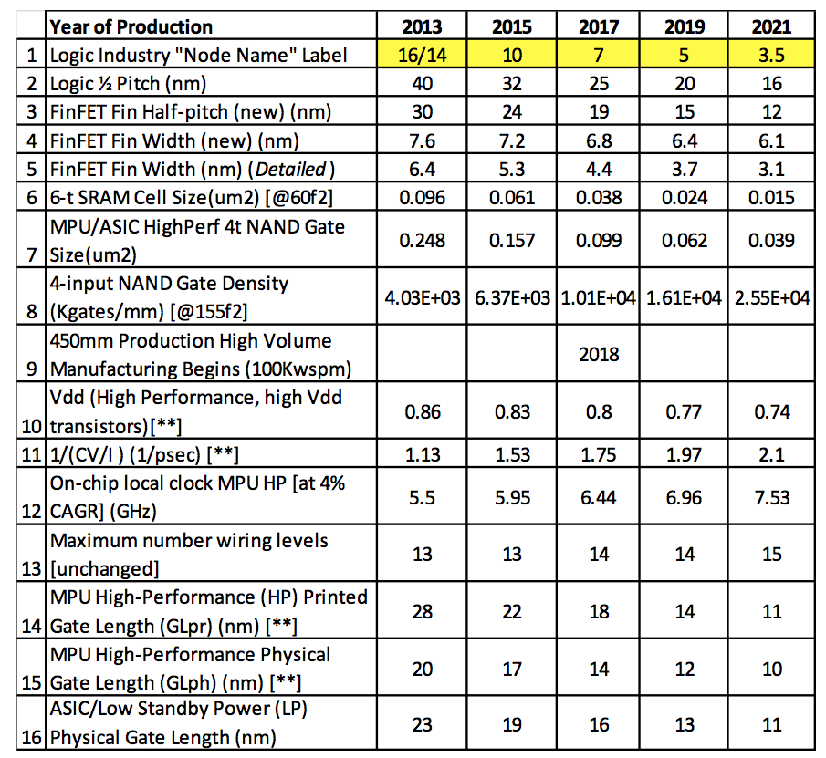
I would love to see an explanation on the differences between the 14nm process and the 16nm process because from what I've found they appear to be the same and it is just a nomenclature thing that allows the process to be referred to as either 14nm or 16nm.
Sakkura
Illustrious
- Aug 22, 2011
- 8,129
- 3
- 37,965
Mousemonkey :
Sakkura :
The AMD slide does say FinFET enables the drive to 16nm and beyond, so eh. These process node numbers are kinda fudged anyway.
I would love to see an explanation on the differences between the 14nm process and the 16nm process because from what I've found they appear to be the same and it is just a nomenclature thing that allows the process to be referred to as either 14nm or 16nm.
They're definitely different. GloFo is license-building on Samsung's 14nm FinFET process, while TSMC have their own 16nm FinFET process. In fact there are more processes available. TSMC had their first-gen 16nm FF, then 16nm FF+ and FFC. Nvidia is using 16FF+ for Pascal. Samsung has 14LPE and 14LPP, of which AMD, by way of GloFo, is using the latter.
There have been some eyes on this, especially when Apple dual-sourced their A9 SOC from TSMC and Samsung. I believe they used the same TSMC 16FF+ as Nvidia is using now, whereas they were using the 14LPE process from Samsung rather than the 14LPP process that AMD is basing Polaris on.
Here is an Anandtech article about the A9. While the comparisons there won't necessarily translate as 14LPE and 14LPP are not the same, at least you get an idea of what's going on.
In theory, you'd expect the same chip design to be 31% larger if built on a 16nm process than on a 14nm process. But it turns out the A9 is only 9% bigger on TSMC 16FF+ than on Samsung 14LPE. So the size difference between these examples of "16nm" and "14nm" is smaller than advertised. If you compare against Intel's 14nm process, that's also quite different in terms of density (see below). But then when you get into the details of it, there are other important aspects than just the dimensions of the transistors.

Mousemonkey
Titan
- Sep 3, 2006
- 59,462
- 17
- 92,965
Sakkura :
Mousemonkey :
Sakkura :
The AMD slide does say FinFET enables the drive to 16nm and beyond, so eh. These process node numbers are kinda fudged anyway.
I would love to see an explanation on the differences between the 14nm process and the 16nm process because from what I've found they appear to be the same and it is just a nomenclature thing that allows the process to be referred to as either 14nm or 16nm.
They're definitely different. GloFo is license-building on Samsung's 14nm FinFET process, while TSMC have their own 16nm FinFET process. In fact there are more processes available. TSMC had their first-gen 16nm FF, then 16nm FF+ and FFC. Nvidia is using 16FF+ for Pascal. Samsung has 14LPE and 14LPP, of which AMD, by way of GloFo, is using the latter.
There have been some eyes on this, especially when Apple dual-sourced their A9 SOC from TSMC and Samsung. I believe they used the same TSMC 16FF+ as Nvidia is using now, whereas they were using the 14LPE process from Samsung rather than the 14LPP process that AMD is basing Polaris on.
Here is an Anandtech article about the A9. While the comparisons there won't necessarily translate as 14LPE and 14LPP are not the same, at least you get an idea of what's going on.
In theory, you'd expect the same chip design to be 31% larger if built on a 16nm process than on a 14nm process. But it turns out the A9 is only 9% bigger on TSMC 16FF+ than on Samsung 14LPE. So the size difference between these examples of "16nm" and "14nm" is smaller than advertised. If you compare against Intel's 14nm process, that's also quite different in terms of density (see below). But then when you get into the details of it, there are other important aspects than just the dimensions of the transistors.
Not quite the same as what I found but interesting nonetheless.
- Jul 15, 2014
- 22,627
- 9
- 60,960


Mousemonkey :
Sakkura :
Mousemonkey :
Sakkura :
The AMD slide does say FinFET enables the drive to 16nm and beyond, so eh. These process node numbers are kinda fudged anyway.
I would love to see an explanation on the differences between the 14nm process and the 16nm process because from what I've found they appear to be the same and it is just a nomenclature thing that allows the process to be referred to as either 14nm or 16nm.
They're definitely different. GloFo is license-building on Samsung's 14nm FinFET process, while TSMC have their own 16nm FinFET process. In fact there are more processes available. TSMC had their first-gen 16nm FF, then 16nm FF+ and FFC. Nvidia is using 16FF+ for Pascal. Samsung has 14LPE and 14LPP, of which AMD, by way of GloFo, is using the latter.
There have been some eyes on this, especially when Apple dual-sourced their A9 SOC from TSMC and Samsung. I believe they used the same TSMC 16FF+ as Nvidia is using now, whereas they were using the 14LPE process from Samsung rather than the 14LPP process that AMD is basing Polaris on.
Here is an Anandtech article about the A9. While the comparisons there won't necessarily translate as 14LPE and 14LPP are not the same, at least you get an idea of what's going on.
In theory, you'd expect the same chip design to be 31% larger if built on a 16nm process than on a 14nm process. But it turns out the A9 is only 9% bigger on TSMC 16FF+ than on Samsung 14LPE. So the size difference between these examples of "16nm" and "14nm" is smaller than advertised. If you compare against Intel's 14nm process, that's also quite different in terms of density (see below). But then when you get into the details of it, there are other important aspects than just the dimensions of the transistors.
Not quite the same as what I found but interesting nonetheless.
Well, they can't be exactly the same. I recall Invalid Error saying there is no standardization for creating a generalized nanometer number. But there definitely are differences, nothing is ever exact.
Martell1977
Splendid
- Oct 26, 2010
- 3,845
- 3
- 24,960
Tripped off quite a discussion and I have to admit, I've been learning a lot about it. I wonder though, if there is any way to know how much difference in the GPU's is due to the difference between 14nm and 16nm, or if there is any measurable difference at all. Regardless, this generation of GPU's is very interesting and the prospect of full desktop level GPU's in laptops is awesome.
I'm waiting for the new mobile lineup from both companies, want to get a rockin' ~$700 laptop, which right now has a 950m GPU. But if the 480 is as good as touted, it looks like the new laptops will be a huge jump in GPU power as well.
I'm waiting for the new mobile lineup from both companies, want to get a rockin' ~$700 laptop, which right now has a 950m GPU. But if the 480 is as good as touted, it looks like the new laptops will be a huge jump in GPU power as well.
Mousemonkey
Titan
- Sep 3, 2006
- 59,462
- 17
- 92,965
Martell1977 :
Tripped off quite a discussion and I have to admit, I've been learning a lot about it. I wonder though, if there is any way to know how much difference in the GPU's is due to the difference between 14nm and 16nm, or if there is any measurable difference at all. Regardless, this generation of GPU's is very interesting and the prospect of full desktop level GPU's in laptops is awesome.
I'm waiting for the new mobile lineup from both companies, want to get a rockin' ~$700 laptop, which right now has a 950m GPU. But if the 480 is as good as touted, it looks like the new laptops will be a huge jump in GPU power as well.
I'm waiting for the new mobile lineup from both companies, want to get a rockin' ~$700 laptop, which right now has a 950m GPU. But if the 480 is as good as touted, it looks like the new laptops will be a huge jump in GPU power as well.
You and me both mate, as for laptops :- http://www.guru3d.com/news-story/rumor-nvidia-to-use-gtx-1070-and-1080-in-laptops.html the mobile GPU may be a thing of the past if that turns out to be true.
- Jun 23, 2014
- 18,256
- 427
- 81,340


Mousemonkey :
Martell1977 :
Tripped off quite a discussion and I have to admit, I've been learning a lot about it. I wonder though, if there is any way to know how much difference in the GPU's is due to the difference between 14nm and 16nm, or if there is any measurable difference at all. Regardless, this generation of GPU's is very interesting and the prospect of full desktop level GPU's in laptops is awesome.
I'm waiting for the new mobile lineup from both companies, want to get a rockin' ~$700 laptop, which right now has a 950m GPU. But if the 480 is as good as touted, it looks like the new laptops will be a huge jump in GPU power as well.
I'm waiting for the new mobile lineup from both companies, want to get a rockin' ~$700 laptop, which right now has a 950m GPU. But if the 480 is as good as touted, it looks like the new laptops will be a huge jump in GPU power as well.
You and me both mate, as for laptops :- http://www.guru3d.com/news-story/rumor-nvidia-to-use-gtx-1070-and-1080-in-laptops.html the mobile GPU may be a thing of the past if that turns out to be true.
That makes perfect sense. With how efficent GPUs are today, why shouldn't a detuned gtx 1070/1080 work in a laptop.
Mousemonkey
Titan
- Sep 3, 2006
- 59,462
- 17
- 92,965
I wouldn't be at all surprised if AMD does the same thing with their new line up as well, then it's just a race to see who will be the first to put their GPU into a smartphone I guess. 😉
- Jun 23, 2014
- 18,256
- 427
- 81,340
Mousemonkey :
I wouldn't be at all surprised if AMD does the same thing with their new line up as well, then it's just a race to see who will be the first to put their GPU into a smartphone I guess. 😉
I'm skeptical about descrete GPUs in smartphones. I think the better route is for the ARM CPUs (like snapdragon) to product IGPUs that are just as powerful as the mainstream GT or low end GTX GPUs.
- Status
- Not open for further replies.
TRENDING THREADS
-

-
-

-
-
 Discussion What's your favourite video game you've been playing?
- Started by amdfangirl
- Replies: 4K
Space.com is part of Future plc, an international media group and leading digital publisher. Visit our corporate site.
© Future Publishing Limited Quay House, The Ambury, Bath BA1 1UA. All rights reserved. England and Wales company registration number 2008885.
 Twitter