News Intel's Patent Details Meteor Lake's 'Adamantine' L4 Cache

Page 3 - Seeking answers? Join the Tom's Hardware community: where nearly two million members share solutions and discuss the latest tech.
Before the L4$ can do its thing, the L3$ has to conclude that it missed. The read/write address also has to get to it over an off-die interface and routing fabric that connects L4$ to everything else. The L3$ adds 36 cycles on top of L2$ latency on Zen 4, a bigger L4$ made on a cheaper process (interposers are made on 12-16nm class processes if that is really where you want to put your L4$) would almost certainly add another 40+ cycles due to the much longer physical roundtrip and extra clocked hops to help cover the distance.
I don't think a L3 cache miss combined with a L4 cache hit will cost the tCPU close to 100 clocks. If thats the case, Intel may forego ADM L4 altogether! I'm think it's gonna be in the ballpark of X3D Vcache. A few dozen cycles at most.

(Just a disclaimer: ADM L4 on MTL is still not confirmed)
 
I don't think a L3 cache miss combined with a L4 cache hit will cost the tCPU close to 100 clocks. If thats the case, Intel may forego ADM L4 altogether! I'm think it's gonna be in the ballpark of X3D Vcache. A few dozen cycles at most.
The reason why AMD's V-cache doesn't add latency to on-die L3$ is because the the V-cache is a straight-up space extension to on-die L3$ and shares the on-die L3$ tag-RAM which is where most of the latency comes from - it takes time to scan a large tag-RAM for an address match.

As for what Adamantine will get used for, Intel's patent puts a lot of emphasis on things like faster boot times, running secure code, buffering GPU-CPU IO and other things that have little or nothing to do with normal application performance. Basically, acting as L4$ doesn't appear to be its primary or even secondary purpose, just one of the many things it could hypothetically be used for in some cases.
Makes sense as latency in the range of 100 clock cycles doesn't make sense for the tCPU. But acting as L3 for the tGPU makes a lot of sense as it might be able to service the tGPU's L2 within 30 - 50 clocks. Might be worth it after all!

(Disclaimer: Assuming ADM L4 on MTL exists)
 
I very much doubt that the L4 cache will have anything to do with cache misses.
It's all about having massive datasets available for the CPU in a more convenient place than the main ram.
That's what benchmarks utilize and it's also what real-life uses.
Look at 7zip, it has a 32Mb dataset in the build in benchmark by default and zen was much better in that benchmark until intel got a big enough cache as well.
And that goes for most things in general, the more of the data you have the closer to the CPU the faster it will go.
Look at x3d game benchmarks compared to non 3xd.
That sounds much more intersting to me, too. Actually I could even see benefits of a scratch pad area that isn't even mapped to RAM (or has a relaxed coherency and snoop requirements) and for exclusive use by say the iGPU or a neural accelerator.

Most cache efficiency deliberations are made on a code or rather CPU data base, local data and arrays, with very chaotic locality and strong dependencies on tags and coherency. But some of the more DSP like workloads could really rip through stuff on this scratch pad area and of course it could also contain compression dictionaries.

The major issue here is administering this special RAM as it's basically a new storage class and current operating systems (libraries and compilers) wouldn't know how to make sense of that. Hmm, security issues could be serious, too. But with HBM tiles similar challenges loom.

So I guess iGPU or iNPU exclusive scratch pads make for the easiest early adoption?
 
Having it as a scratch pad for special purpose applications introduces too many issues.

(1) App might require a special API and/or I/O instructions to access ADM which negates the entire purpose.
(2) Even if it's memory mapped to an address range, it still requires special code which again negates the purpose.

Instead, it's expected be part of the cache hierarchy (probably tGPU) without requiring any special purpose hardware or software. Works out of the box.
 
  • Like
Reactions: bit_user
Having it as a scratch pad for special purpose applications introduces too many issues.

(1) App might require a special API and/or I/O instructions to access ADM which negates the entire purpose.
(2) Even if it's memory mapped to an address range, it still requires special code which again negates the purpose.

Instead, it's expected be part of the cache hierarchy (probably tGPU) without requiring any special purpose hardware or software. Works out of the box.
These are all things that intel already works on for their server xeon CPUmax although I do think that this cache will be transparent and just show up as a big cache that every software that can use a big cache will be able to use.
 
Having it as a scratch pad for special purpose applications introduces too many issues.

(1) App might require a special API and/or I/O instructions to access ADM which negates the entire purpose.
(2) Even if it's memory mapped to an address range, it still requires special code which again negates the purpose.

Instead, it's expected be part of the cache hierarchy (probably tGPU) without requiring any special purpose hardware or software. Works out of the box.
Just to clarify, when I said "not mapped to RAM", I meant not with DRAM backing, it obviously would have to be memory mapped because they wouldn't want to create an ISA extension just for that.

But I'm pretty sure there are still some bits somewhere on the page tables, which would keep the memory controller from trying to write this back to DRAM or snooping for coherency with other bus masters. And that's not too far from what you're saying. I'd guess.

The attraction of having stacks of DRAM or HBM on-die is simply too great to ignore, even after Intel's Xeon Phi failures and its HMC or MCDRAM: the von Neumann bottleneck isn't going anywhere so if bandwidth is the only way to make more things happen, you'll have to widen the paths for at least some of the data.
 
These are all things that intel already works on for their server xeon CPUmax although I do think that this cache will be transparent and just show up as a big cache that every software that can use a big cache will be able to use.
Intel's patent lists about a dozen non-cache uses for the thing. It'll likely get partitioned between multiple things from IGP caching to kernel scratchpad and high-security memory for DRM, TPM, etc.
 
  • Like
Reactions: bit_user
Intel's patent lists about a dozen non-cache uses for the thing. It'll likely get partitioned between multiple things from IGP caching to kernel scratchpad and high-security memory for DRM, TPM, etc.
I'm sure that it will be partitioned for all of these things, that doesn't mean that there will be none left over to act as a basic cache.
I don't think intel has to mention basic cache usage in the patent to use it as basic cache in the final product.
 
I don't think intel has to mention basic cache usage in the patent to use it as basic cache in the final product.
While it doesn't have to, the fact that the patent puts 90+% of the emphasis on other stuff looks like a strong indication that acting as a flat extra cache tier for the CPU is not intended to be its primary purpose even by a long shot.

Adding 10ns of latency to all L3$ misses with L4 is a bit like like adding +30 to CAS on DDR5-6000. Applications with little additional data locality between L3$ and L4$ sizes will suffer substantial performance penalties. For performance reasons, it will likely be necessary for applications to mark memory pages they wish to (not) be L4-cacheable.
 
I don't think a L3 cache miss combined with a L4 cache hit will cost the tCPU close to 100 clocks. If thats the case, Intel may forego ADM L4 altogether!
Something to consider is that we tend to think in terms of best-case latency. However, when the SoC is under high load, the queues will fill up and the typical latency will actually be much greater. So, even if the latency for L4 is as high as @InvalidError estimates, it could still be a win vs. going all the way out to DRAM.

I'd love it if people doing these micro-benchmarks could start adding some worst-case analysis, to figure out how bad it can get, in situations of high memory contention.
 
That sounds much more intersting to me, too. Actually I could even see benefits of a scratch pad area that isn't even mapped to RAM (or has a relaxed coherency and snoop requirements) and for exclusive use by say the iGPU or a neural accelerator.
I don't think Intel would do that. The GPU has its own scratchpad memory, with relaxed coherency. For any memory visible to the CPU cores, it either needs to be treated as uncached, making it of limited usefulness to the CPU, or fully supporting x86's strong memory ordering. There's no real in-between.

some of the more DSP like workloads could really rip through stuff on this scratch pad area
Yes, and that's why DSPs and GPUs tend to have scratchpad memory. For general-purpose CPUs, the problem is that you'd have to flush your scratchpad as part of your thread context. Since paging in & out your scratchpad would get expensive, it's easier just to rely on caches.

The major issue here is administering this special RAM as it's basically a new storage class and current operating systems (libraries and compilers) wouldn't know how to make sense of that. Hmm, security issues could be serious, too.
If the scratch pad were treated as thread-private, then it would be fine. No different than registers, really.

But with HBM tiles similar challenges loom.
I disagree. HBM should look like main memory, except the OS just needs to be aware that it's faster and therefore needs to actively migrate pages in and out of it.

These are all things that intel already works on for their server xeon CPUmax
That's different both in magnitude and kind. This supposed L4 cache will be 2-3 orders of magnitude smaller. I think the OS will be primarily tasked with managing HBM, but I concede that I have yet to see details of how it's meant to work. In contrast, I expect ADM will be hardware-managed.

The attraction of having stacks of DRAM or HBM on-die is simply too great to ignore, even after Intel's Xeon Phi failures and its HMC or MCDRAM: the von Neumann bottleneck isn't going anywhere so if bandwidth is the only way to make more things happen, you'll have to widen the paths for at least some of the data.
It's not just a bandwidth problem, but also a matter of energy-efficiency. Data movement is energy-intensive.
 
Last edited:
  • Like
Reactions: SiliconFly
the fact that the patent puts 90+% of the emphasis on other stuff looks like a strong indication that acting as a flat extra cache tier for the CPU is not intended to be its primary purpose even by a long shot.
I'd suggest you should be reading patents differently than design documents or whitepapers. Maybe the patent doesn't focus on it as a cache, because that would simply be indefensible.
 
I'd suggest you should be reading patents differently than design documents or whitepapers. Maybe the patent doesn't focus on it as a cache, because that would simply be indefensible.
With the number of patent lawsuits over "same old crap we did over postal service, phone or in-person but over e-mail, IP, Twitter, pigeons, etc." you cannot downplay the obvious stuff too much when you add alternate functionality unless the obvious function is of limited importance.
 
With the number of patent lawsuits over "same old crap we did over postal service, phone or in-person but over e-mail, IP, Twitter, pigeons, etc." you cannot downplay the obvious stuff too much when you add alternate functionality unless the obvious function is of limited importance.
What would the alternate functionality be in the case of them using cache as cache?!
If there was anything then they will have patented it with broadwell, nobody needs to patent the same thing multiple times.
 
What would the alternate functionality be in the case of them using cache as cache?!
If there was anything then they will have patented it with broadwell, nobody needs to patent the same thing multiple times.
Patents have to be pedantically inclusive either explicitly or by generalization if you don't want to get screwed over by someone else patenting fundamentally the same thing with the obvious omissions put in.
 
While it doesn't have to, the fact that the patent puts 90+% of the emphasis on other stuff looks like a strong indication that acting as a flat extra cache tier for the CPU is not intended to be its primary purpose even by a long shot.

Adding 10ns of latency to all L3$ misses with L4 is a bit like like adding +30 to CAS on DDR5-6000. Applications with little additional data locality between L3$ and L4$ sizes will suffer substantial performance penalties. For performance reasons, it will likely be necessary for applications to mark memory pages they wish to (not) be L4-cacheable.
Very true. ADM acting as a L4 cache will introduce too steep a penalty. Looks like it's destined for the tGPU primarily.
 
Something to consider is that we tend to think in terms of best-case latency. However, when the SoC is under high load, the queues will fill up and the typical latency will actually be much greater. So, even if the latency for L4 is as high as @InvalidError estimates, it could still be a win vs. going all the way out to DRAM.

I'd love it if people doing these micro-benchmarks could start adding some worst-case analysis, to figure out how bad it can get, in situations of high memory contention.
Actually, by nature, ADM L4 adds significant latency. This latency becomes a huge issue when cache misses exceeds cache hits. So, when the cache hits are low, the significantly increased DRAM access time will seriously degrade tCPU performance. ADM working as L4 seems very unlikely.

Or do they have some kinda new architecture where L4 cache-controller & DRAM memory-controller are queried simultaneously? (Meaning, not waiting for a L4 cache-miss to query DRAM). Not very ideal, but has the potential to increase performance at the cost of little bit more power.
 
Or do they have some kinda new architecture where L4 cache-controller & DRAM memory-controller are queried simultaneously? (Meaning, not waiting for a L4 cache-miss to query DRAM). Not very ideal, but has the potential to increase performance at the cost of little bit more power.
From the patent, it seems far more likely that the "L4$" will effectively act as a NUMA region partitioned between different uses by its drivers/OS instead of as conventional cache.
 
From the patent, it seems far more likely that the "L4$" will effectively act as a NUMA region partitioned between different uses by its drivers/OS instead of as conventional cache.
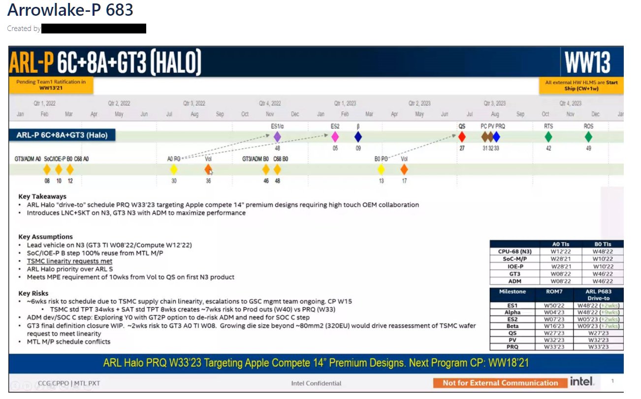
This was leaked a long while ago. And at that time, many didn't notice. It all makes sense now!

FMOhNpmWUAAV_WR.jpg:large
If we read it carefully, it clearly says ADM is paired with GT2P!!! Thats the tGPU in MTL-P

Also says with LNC, ADM is paired with GT3.

Thats cool! :blush:
 
Last edited:
  • Like
Reactions: bit_user
Actually, by nature, ADM L4 adds significant latency. This latency becomes a huge issue when cache misses exceeds cache hits. So, when the cache hits are low, the significantly increased DRAM access time will seriously degrade tCPU performance. ADM working as L4 seems very unlikely.
Read latency can be masked by prefetching and speculative loads.

Or do they have some kinda new architecture where L4 cache-controller & DRAM memory-controller are queried simultaneously?
I was thinking about this, but it would only work if you can invalidate the memory transaction should the contents of L4 be dirty. Remember that if it's working as a system-level cache, then it needs to be kept coherent.

Not very ideal, but has the potential to increase performance at the cost of little bit more power.
This is exactly why I think they won't do it. With Meteor Lake being mobile-focused, power-savings are very important.
 
Came across a new rumor. Note: It's just a rumor/speculation based on an assumption.

Even though a leaked Intel slide suggested that ADM L4 will be paired with tGPU, I recently came across a detailed analysis that seems to suggest that ADM L4 might not be paired directly with the tGPU, but with the SoC tile to enable advanced idle states that helps MTL to power-off the CPU tile & GPU tile at the *SAME TIME* while idling. That'd be wow!
 
ADM L4 might not be paired directly with the tGPU, but with the SoC tile to enable advanced idle states that helps MTL to power-off the CPU tile & GPU tile at the *SAME TIME* while idling. That'd be wow!
If the display is in power-saving mode, then I can understand powering down the GPU. Obviously, they're going to support powering down the CPU tile, with those 2x LPE cores in the SoC tile.

Now, what any of this has to do with ADM is very unclear to me. In mobile SoCs, they tend to power down system-level cache in low-power states. That seems to be the reverse of what you're saying.
 
Also, a while ago, that idiot MLID suggested that the ADM L4 will be separate tile between the base tile and the substrate. And i was scratching my head why on earth Intel would do something stupid like this for no apparent advantage.

After digging deeper, it's now clear that the ADM L4 is part of the base tile which is now confirmed to be an active interposer with logic & sram (and naturally tsvs). Might be produced on Intel 16 or Intel 7.

Which gets me to believe that there are going to be two versions. The lower end core ultra 3 will have a passive interposer base tile (with no L4 cache) made using Intel 16. And the mid-range core ultra 5 will have an active interposer base tile with L4 cache made using Intel 7 for improved efficiency.
 
Last edited:
If the display is in power-saving mode, then I can understand powering down the GPU. Obviously, they're going to support powering down the CPU tile, with those 2x LPE cores in the SoC tile.

Now, what any of this has to do with ADM is very unclear to me. In mobile SoCs, they tend to power down system-level cache in low-power states. That seems to be the reverse of what you're saying.
Seems L4 is ultra power efficient and doesn't need to be powered down. Instead, in the new low-power state, when the frame buffer doesn't need to be updated, the video memory can be buffered in the cache while idling and the tGPU can be powered-off as well.