News Nvidia GeForce RTX 3080 Founders Edition Review: A Huge Generational Leap in Performance
Page 6 - Seeking answers? Join the Tom's Hardware community: where nearly two million members share solutions and discuss the latest tech.
You are using an out of date browser. It may not display this or other websites correctly.
You should upgrade or use an alternative browser.
You should upgrade or use an alternative browser.
nofanneeded
Respectable
- Sep 29, 2019
- 1,541
- 248
- 2,090


Citations, please?
RTX 3080 should be benchmarked for 8K ... If it is 20% slower than 3090 it should game at normal or high (not ultra) with 60 fps .. and we NEED TO KNOW.
Tomshardware should Benchmark it
That's not a citation. That's an advertising/promotional gimmick, and, with particularly selected (re)actors. digitalgriffin already explained this.
So, at least you're proving that you have no sources. I meant actual tests, reviews, etc., like the sort of thing you're demanding from Tom's Hardware . . NOT videos of people reacting to it.
Hell, you're complaining that it's not benchmarked, and you're using a gimmick video to PROVE that 8K@60 is already here? Which is it? Are there benchmarks to prove it's already here, or not?
nofanneeded
Respectable
- Sep 29, 2019
- 1,541
- 248
- 2,090
That's not a citation. That's an advertising/promotional gimmick, and, with particularly selected (re)actors. digitalgriffin already explained this.
So, at least you're proving that you have no sources. I meant actual tests, reviews, etc., like the sort of thing you're demanding from Tom's Hardware . . NOT videos of people reacting to it.
Hell, you're complaining that it's not benchmarked, and you're using a gimmick video to PROVE that 8K@60 is already here? Which is it? Are there benchmarks to prove it's already here, or not?
Nvidia CEO said it reached 60fps on 8K . Go sue him !
My source is Nvidia CEO. and all what I am asking is for Tomshardware to Benchmark it and see how TRUE it is . how do we know he is truthful or not ? we BENCHMARK !
what is your problem exactly ? cant you see that I want it to be BENCHMARKED to SEE if Nvidia CEO is telling the truth or not ?
So, your "proof" of performance is the word of the guy who's motivated to show his own products in a better light?
Well, I say 8k@60 isn't even close to being a thing. You can tell it's true because you have my word for it.
That's not a source. That's just a guy talking. There's no full test . . the kind you're demanding from this site.
My problem is that you stated that 8K60 is already here - insisting that people should cater to YOUR beliefs and cave to YOUR demands for testing that serves no practical purpose.
I mean, go buy it if you want, you're free to do so. Just don't try to sell everyone else on the idea that this video that amounts to an advertising blurb constitutes proof of your claims that 8k gaming is here in any practical way.
drivinfast247
Glorious
- May 29, 2018
- 7,845
- 1,646
- 47,940


This is a simple problem to solve. Go buy a 8k display and 3080 and test it yourself.Nvidia CEO said it reached 60fps on 8K . Go sue him !
My source is Nvidia CEO. and all what I am asking is for Tomshardware to Benchmark it and see how TRUE it is . how do we know he is truthful or not ? we BENCHMARK !
what is your problem exactly ? cant you see that I want it to be BENCHMARKED to SEE if Nvidia CEO is telling the truth or not ?
nofanneeded
Respectable
- Sep 29, 2019
- 1,541
- 248
- 2,090
So, your "proof" of performance is the word of the guy who's motivated to show his own products in a better light?
Well, I say 8k@60 isn't even close to being a thing. You can tell it's true because you have my word for it.
That's not a source. That's just a guy talking. There's no full test . . the kind you're demanding from this site.
My problem is that you stated that 8K60 is already here - insisting that people should cater to YOUR beliefs and cave to YOUR demands for testing that serves no practical purpose.
I mean, go buy it if you want, you're free to do so. Just don't try to sell everyone else on the idea that this video that amounts to an advertising blurb constitutes proof of your claims that 8k gaming is here in any practical way.
my original post is about proving it and asking tomshardware to benchmark it to prove it. I never said it is proved ,
and your problem is that you picking words from my posts and leaving the whole context . my context is clear ! I want proof ! I want benchmark.
You left the whole context and cut out "60 fps is here" to play around it ? because I did not say "Nvidia said it is here" ?
well , sorry you are flaming , because the context of my post is clear. I was not trying to provr it is here , I was ASKING tomshardware to see if it is true or not by benchmarks. . you are just trying to look for in between the lines not clear statement and base you attacks on them.
This is my last reply to you.
nofanneeded
Respectable
- Sep 29, 2019
- 1,541
- 248
- 2,090
This is a simple problem to solve. Go buy a 8k display and 3080 and test it yourself.
Why do we pay in ads for tomshardware to test hardware before we buy then ?
JarredWaltonGPU
Splendid
- Feb 21, 2020
- 2,891
- 4,701
- 23,570


Yeah, and the funny thing is the only proper 8K displays right now are TVs. The 8K Dell requires two cables, which means the GPU sees it as two half-8K displays and that potentially causes some odd behavior. Anyway, I'm going to test 8K via DSR (Dynamic Super Resolution). It's not totally the same -- DSR I think is usually 3-5% slower due to a bit of extra work the GPU has to do to render and then scale the result -- but it will be 'close enough.' Of course without a 65-inch 8K display, I'm not getting the proper 8K experience so I can't do jaw drops and "holy ****!" faces for a promotional video.This is a simple problem to solve. Go buy a 8k display and 3080 and test it yourself.
JarredWaltonGPU
Splendid
- Feb 21, 2020
- 2,891
- 4,701
- 23,570
The outside edge has mostly memory controllers on Ampere and Turing. It's interesting to see how they've been shifted around for GA102 vs. TU102, plus the whole middle section of TU102 has always been a bit of a mystery to me. Is it cache on the left and right? And the very center block -- WTF is that?In the Tu102 the SMs take up roughly the same amount of space: ~55%.
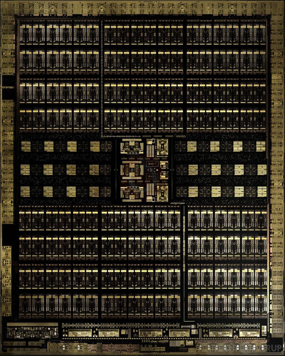
It's interesting how we can visibly see the difference between the two processes. The Samsung produced die is more squarish, whereas the TSMC die has a definite preferred direction.
Anyway, there doesn't seem to be any extra functional units in Turing that would accord for the extra transistors. I think it's down to the process.
Not sure what the things around the perimeter are. They're proportionally bigger in Ampere.
GA102 is far more sensible to decipher, for me anyway. I guess the bottom section of GA102 is still murky, though. There's obviously stuff for video controllers somewhere, along with the ROPs and TMUs and what have you. Nvidia sadly doesn't generally provide a clear explanation of what the various functional units are for the chip shots.
- Dec 30, 2016
- 21,694
- 5,772
- 104,690


That TV has an advertised 6ms response time. That, combined with it needing 2 cables and the other latency mumbo-jumbo I'm not familiar with, tells me that no, 8K 60 is NOT here, except in a controlled environment...The 8K Dell
Hmm, a controlled environment...
TerryLaze
Titan
- May 9, 2016
- 10,923
- 3,115
- 76,440


That is what you are doing,when you say that the CEO said it than provide a link to were you read or seen it so we can see what he actually said.You left the whole context and cut out "60 fps is here" to play around it ?
Far as I know these new cards have hdmi 2.1 which means that they can send one single 8k picture to a monitor/tv instead of having to do a composite of 4 4k pictures, if he said only that and you didn't understood it properly then that doesn't need any benchmarking, if it has hdmi 2.1 then it can do 8k 60FPS.
This does not mean ultra gaming unless he said specifically 8k 60 FPS ultra gaming, if he didn't add the ultra gaming part then the ultra gaming part is not part of what he said.
Chung Leong
Reputable
- Dec 6, 2019
- 494
- 193
- 4,860
The outside edge has mostly memory controllers on Ampere and Turing.
Ah, that makes sense. Processing the PAM4 signaling would require more circuitry.
It's interesting to see how they've been shifted around for GA102 vs. TU102, plus the whole middle section of TU102 has always been a bit of a mystery to me. Is it cache on the left and right?
The cache would be too small relative to the overall size for us to pick out. I have no idea what those things could be.
And the very center block -- WTF is that?
Those are probably clusters of RT cores. In the GA102 die there are seven of them, which sort of match the reported 84 RT cores. So the 3080 can withstand one faulty RT cluster and still have half a cluster disabled for market segmentation purpose. Yield should be massively better than Turing.
GA102 is far more sensible to decipher, for me anyway.
Samsung's process provides a lot of flexibility. You can lay things out on the silicon the way you want. It's error-prone as features are lithed and etched in four separate steps. Any misalignment between steps would destroy the whole wafer. The process adopted by TSMC and Intel doesn't have this problem, but then you have to lay out your chip in a very specific way.
Processes have trade-offs. If you're making a CPU, you get a lot of benefits from denser caches and higher frequency. You don't get those when you're making a GPU. A GPU is a bunch of weak processors that win through sheer number. It makes absolutely perfect sense, if you think about it, to use the same process to make high-end GPUs as for making chips in low-end, cheap-o phones sold in India.
alithegreat
Distinguished
- Aug 15, 2013
- 72
- 1
- 18,640

Hello,
I believe the power demanded by the card is too much and it's not emphasised enough. Performance per watt is always bad on high end cards but there is still 3090 thing which will be worse possibly. Will we get a performance per watt chart after you review partner cards and such?
I hope AMD doesn't do the same, otherwise everyone will be paying for power supplies and more bills. These cards cost will be way higher than first realized.
Thanks,
- Dec 30, 2016
- 21,694
- 5,772
- 104,690
TechPowerUp did it for the 3080, if you're interested: https://www.techpowerup.com/review/nvidia-geforce-rtx-3080-founders-edition/35.htmlI believe the power demanded by the card is too much and it's not emphasised enough. Performance per watt is always bad on high end cards but there is still 3090 thing which will be worse possibly. Will we get a performance per watt chart after you review partner cards and such?
JarredWaltonGPU
Splendid
- Feb 21, 2020
- 2,891
- 4,701
- 23,570
Would it? I mean, the cache on Intel's CPUs is extremely obvious. You get huge blocks of 'easy' transistor logic compared to the mess that is GPU cores. GPU ALUs end up being very small but lots of them, so you can easily spot all of those -- but the shader cores should be very close to some L1/L2 cache. You don't want to fetch data from the other end of chip I don't think. Still, I'm not at all sure what the various middle blocks are on TU102, and the same goes for the lower/middle part of GA102.Ah, that makes sense. Processing the PAM4 signaling would require more circuitry.
The cache would be too small relative to the overall size for us to pick out. I have no idea what those things could be.
I don't think so. There are 48 square 'blocks' in the bottom section of GA102. That doesn't match GPCs, RTs, ROPs, or anything really. It could just be miscellaneous logic for routing data. Furthermore, the SMs are supposed to contain 64 FP32 CUDA, 64 FP32/INT CUDA, 4 Tensor, 1 RT, and some L1$/shared memory. The TPCs are supposed to have L2 cache, ROPS, Texture Units, and the Polymorph engine. So, with that in mind, here's my 'guess' on the GA102 die shot from Nvidia. (The top-right and bottom areas are the major unknowns -- especially that chunk just above the very bottom where I assume the video interfaces and such are located).Those are probably clusters of RT cores. In the GA102 die there are seven of them, which sort of match the reported 84 RT cores. So the 3080 can withstand one faulty RT cluster and still have half a cluster disabled for market segmentation purpose. Yield should be massively better than Turing.

Samsung's process provides a lot of flexibility. You can lay things out on the silicon the way you want. It's error-prone as features are lithed and etched in four separate steps. Any misalignment between steps would destroy the whole wafer. The process adopted by TSMC and Intel doesn't have this problem, but then you have to lay out your chip in a very specific way.
Processes have trade-offs. If you're making a CPU, you get a lot of benefits from denser caches and higher frequency. You don't get those when you're making a GPU. A GPU is a bunch of weak processors that win through sheer number. It makes absolutely perfect sense, if you think about it, to use the same process to make high-end GPUs as for making chips in low-end, cheap-o phones sold in India.
Chung Leong
Reputable
- Dec 6, 2019
- 494
- 193
- 4,860
Furthermore, the SMs are supposed to contain 64 FP32 CUDA, 64 FP32/INT CUDA, 4 Tensor, 1 RT, and some L1$/shared memory.
It wouldn't make sense though to spread the RT cores among the SMs, since they're coupled more to each other than to the shaders. Whereas the SMs each handle a small part of the scene (a triangle or a pixel), all RT cores uses the BVH of the full scene.
My guess is that the RT cores are housed in the clusters under the SMs along with the L2 cache (that bright rectangle). To the RT cores the L2 would actually be L1.
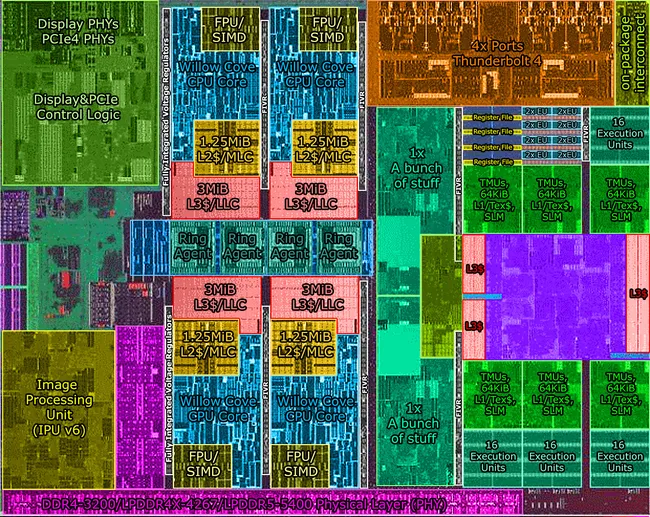
The stuff below reminds me of the "a bunch of stuff" block on the Tiger Lake die.
JarredWaltonGPU
Splendid
- Feb 21, 2020
- 2,891
- 4,701
- 23,570
So here's the big question: are the RT and Tensor cores part of the SMs, as Nvidia says in its architecture whitepaper, or are they located somewhere else?It wouldn't make sense though to spread the RT cores among the SMs, since they're coupled more to each other than to the shaders. Whereas the SMs each handle a small part of the scene (a triangle or a pixel), all RT cores uses the BVH of the full scene.
My guess is that the RT cores are housed in the clusters under the SMs along with the L2 cache (that bright rectangle). To the RT cores the L2 would actually be L1.
The stuff below reminds me of the "a bunch of stuff" block on the Tiger Lake die.
I have to assume they're in the SMs, based on the counts and everything else we know. If the RT cores were separated out from the main SMs, turning on ray tracing functions would make it more costly (latency) to pass data from the RT cores to the shader cores and vice versa, requiring a lot of extra routing of data -- and they'd be away from the L1 cache and even L2 cache. Also, we have the past three generations of Nvidia 102 chips:
GP102: https://tpucdn.com/gpu-specs/images/g/798-die-shot.jpg
TU102: https://tpucdn.com/gpu-specs/images/g/813-die-shot.jpg
GA102: https://tpucdn.com/gpu-specs/images/g/930-cgi-die-shot.jpg
Each chip has a similar area whose purpose isn't fully understood. Since GP102 didn't have RT or Tensor cores, obviously the middle horizontal chunk isn't used for those functions on Pascal. Then the same area on Turing would still be doing basically whatever it did with Pascal -- just more of it. And GA102 moves that section to the bottom due to changes in lithography and architecture.
So my take is that the 'unknown' stuff for caching, memory routing, or whatever else ... but that the RT cores aren't in that area and are within the SMs, as Nvidia has said in their block diagrams and such. Something else I didn't mention before is the video blocks in each of the GPUs also has stuff for NVENC/NVDEC, which probably takes up a modest chunk of die space.
The difficulty is that Nvidia has never provided a similar die shot to the above for things like GP104, TU104, or GA104. But we do have this:
View: https://www.flickr.com/photos/130561288@N04/48116463052/in/photostream/
Deciphering that shot is far more difficult, sadly. If anyone has a good link to a TU104 (or GP104) die shot, post it here. 🙂
cryoburner
Judicious
- Oct 8, 2011
- 5,790
- 1,405
- 34,840


The 3090 will undoubtedly draw more power than the 3080, but it could be similar, or perhaps even slightly more efficient on a performance-per-watt basis. It has 20% more active cores, but only around a 10% higher TDP, so I would expect it to run into power limits and typically operate at lower boost clocks as a result. That will likely mean it won't be getting 20% more performance though, and some review leaks going around are suggesting closer to 10% more performance than a 2080, more or less in line with the difference in TDP. Some of that extra power will be going to the extra memory chips too though, which will likely be sitting around mostly unused in games for quite some time to come.I believe the power demanded by the card is too much and it's not emphasised enough. Performance per watt is always bad on high end cards but there is still 3090 thing which will be worse possibly. Will we get a performance per watt chart after you review partner cards and such?
Chung Leong
Reputable
- Dec 6, 2019
- 494
- 193
- 4,860
I have to assume they're in the SMs, based on the counts and everything else we know. If the RT cores were separated out from the main SMs, turning on ray tracing functions would make it more costly (latency) to pass data from the RT cores to the shader cores and vice versa, requiring a lot of extra routing of data -- and they'd be away from the L1 cache and even L2 cache. Also, we have the past three generations of Nvidia 102 chips:
There shouldn't be all that much traffic between the SM and the RT cores. Nvidia claims 10 gigarays per second on the 2080 Ti. That's 2.3 million rays per core. Divide the game clock by this number yields 670 cycles. A ray intersection search is an expensive operation even with dedicated hardware. I imagine a RT core would spend most of its time waiting for different parts of the BVH tree to transfer from VRAM. Effective caching is key to performance. Spreading out the RT cores is detrimental to that with bringing any clear benefit.
JarredWaltonGPU
Splendid
- Feb 21, 2020
- 2,891
- 4,701
- 23,570
FYI, I have asked my Nvidia contacts about this, and they confirm that the RT cores truly are part of the SMs. That 'unknown' area is most likely related to cache, the internal bus, and other elements. Also, the Nvidia-provided die shots should not be taken as 100% accurate representations of how those die look and how they're laid out. "More like 70%," apparently with some things changed to protect trade secrets, and some things are just enhanced to make it look more legible. It's more like a high level view of the chip layout and not an actual scan of the chip.There shouldn't be all that much traffic between the SM and the RT cores. Nvidia claims 10 gigarays per second on the 2080 Ti. That's 2.3 million rays per core. Divide the game clock by this number yields 670 cycles. A ray intersection search is an expensive operation even with dedicated hardware. I imagine a RT core would spend most of its time waiting for different parts of the BVH tree to transfer from VRAM. Effective caching is key to performance. Spreading out the RT cores is detrimental to that with bringing any clear benefit.
cryoburner
Judicious
- Oct 8, 2011
- 5,790
- 1,405
- 34,840
While I could see why they might potentially do that, it seems like any company with the ability to manufacture their own graphics chips would also have the ability to X-ray and otherwise tear-down their competitor's hardware without the need for analyzing marketing slides. I suppose it could slow them down if they didn't have access to the hardware yet though. But if I had to guess, all these companies likely have informants working for their competitors to keep them up to date on what the competition has planned....apparently with some things changed to protect trade secrets...
"And last but not least, there's no VirtualLink port this round — apparently, VirtualLink is dead. RIP. "
The link is leading to an unrelated page about the best processors 2020. I searched for "virtual" in that article and there were no results, so I believe the link is wrong.
The link is leading to an unrelated page about the best processors 2020. I searched for "virtual" in that article and there were no results, so I believe the link is wrong.
Avro Arrow
Splendid
- Nov 12, 2009
- 4,282
- 1,434
- 26,090


Jarred, I'll start by saying that your review is absolutely spectacular! You have definitely outdone yourself!
I do have a comment to make but it's not about your review, it's about the product itself. You were saying something about the VRAM that I 100% agree with but there is a problem with our kind of thinking:
"If you're worried about 10GB of memory not being enough, my advice is to just stop. Ultra settings often end up being a placebo effect compared to high settings — 4K textures are mostly useful on 4K displays, and 8K textures are either used for virtual texturing (meaning, parts of the texture are used rather than the whole thing at once) or not used at all. We might see games in the next few years where a 16GB card could perform better than a 10GB card, at which point dropping texture quality a notch will cut VRAM use in half and look nearly indistinguishable. "
On a "FLAGSHIP" card like this that is hailed as a card that's specifically for gaming at 2160p, should people have to turn their textures down because nVidia didn't give the card the 12-16GB of VRAM that it should have? Sure, it doesn't matter, I agree with that, but I also think that nVidia shouldn't have made it necessary because this is their "FLAGSHIP" card. Your thoughts?
hotaru.hino
Glorious
- Sep 1, 2020
- 9,805
- 3,567
- 46,090


My guess is the unknown stuff is the equivalent of the front-end of a CPU, i.e., the instruction scheduling and whatnot. If we tried to map the die to the simpler looking block diagrams, the GigaThread engine is the one thing that sticks out to me.So my take is that the 'unknown' stuff for caching, memory routing, or whatever else ... but that the RT cores aren't in that area and are within the SMs, as Nvidia has said in their block diagrams and such.
I'm sure you know this, but for anyone else: NVIDIA didn't make their scheduler purely software based. All they did was remove the dependency checking and instruction reordering in the scheduler since NVIDIA figured operations wer deterministic enough to figure that out in software without much penalty.
TRENDING THREADS
-

-
-

-

-
 Discussion What's your favourite video game you've been playing?
- Started by amdfangirl
- Replies: 4K
-
Space.com is part of Future plc, an international media group and leading digital publisher. Visit our corporate site.
© Future Publishing Limited Quay House, The Ambury, Bath BA1 1UA. All rights reserved. England and Wales company registration number 2008885.
 Twitter