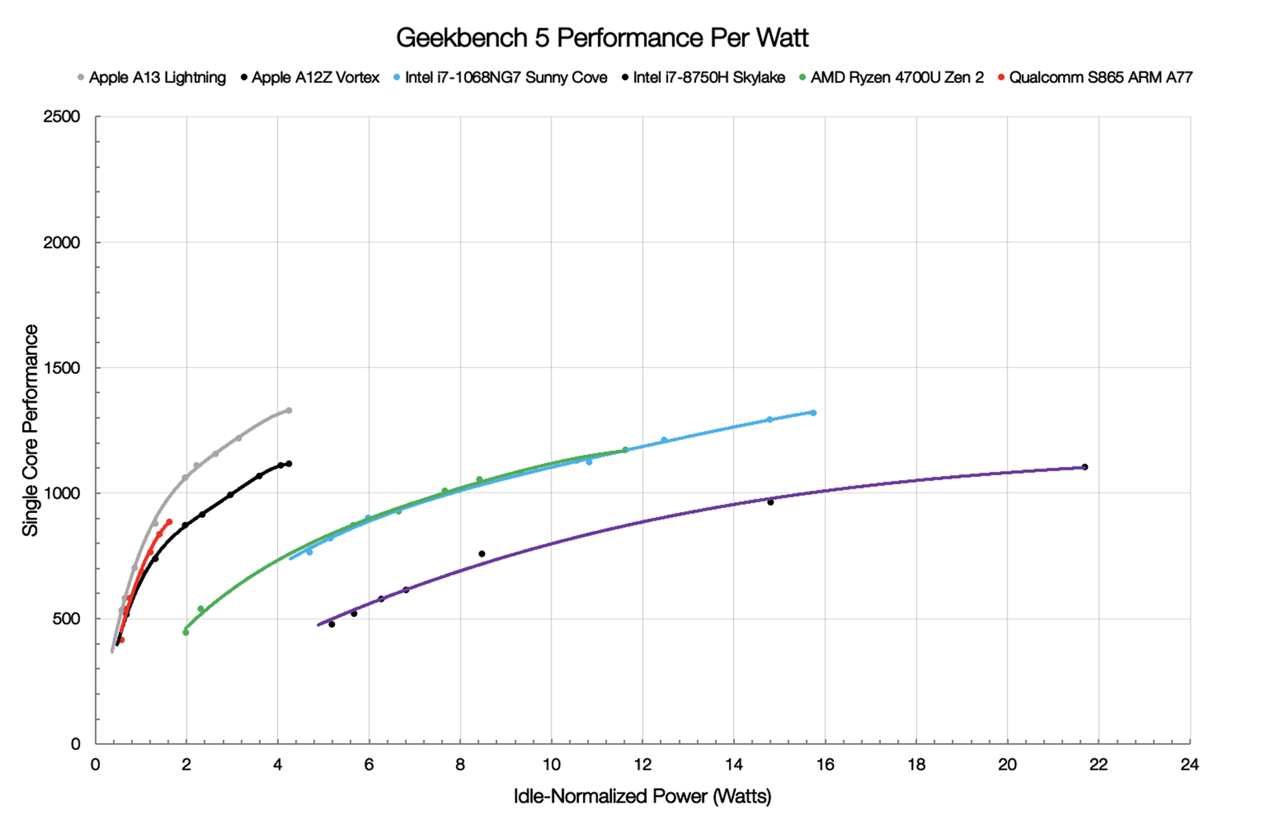
Long time since I posted but it seems it's needed again.
Firstly there is no such thing as CISC, there is RISC and not-RISC, or specifically designs that follow the RISC philosophy and design's that don't. The RISC design philosophy is simply that all instructions are the exact same size and take exactly one cycle to execute. Those two concepts, when taken together, enable
much simpler pipeline and scheduling. Now not everyone followed those requirements exactly, but the idea is generally followed by every design these days.
About x86, there hasn't been a pure x86 CPU designed in decades now. Intel and AMD CPU's are internally RISC CPU's that use an instruction decoder to convert x86 instructions into Load/Store RISC instructions, schedule those instructions on internal ALU/AGU/MMU units, then return the result to the CPU stack for the next instruction to use. Intel's current uArch has 4 ALU's per code along with a bunch of other special purpose units.
https://en.wikichip.org/wiki/intel/microarchitectures/coffee_lake
In the RISC world an execution instruction can only go register to register, we need to load (read) our values into the register from memory and store (write) the output back to memory. x86 on the other hand allows memory address's to be used as a source for many instructions, requiring several cycles to execute the instruction.
ADD AX C800H (add the value at memory address C800H to the BX register and output in the AX register)
MOV 4000H AX (copy the output to memory address 4000H)
that would translate into
LOAD R1 C800H
ADD R1 R2
STORE R2 4000H
This can also be combined as,
ADD 4000H C800H (add the value at C800H to the value at 4000H and store at 4000H)
that's
LOAD R1 4000H
LOAD R2 3800H
ADD R1 R2
STORE R1 4000H
Back when memory was super expensive saving space by having large multi-purpose instructions was thought to be important. These instructions would take up less space in memory and require less machine code to execute. When memory got much cheaper the RISC design philosophy came about as a way to reduce the complexity of the instruction scheduler on the CPU.
Agner has a list of how long each instruction type takes on Intel and AMD architectures.
https://www.agner.org/optimize/instruction_tables.pdf
We can see that most register to register instructions unsurprisingly take 1 CPU cycle to execute, while those involving memory address's take a few more as they need to first be broken into separate read and write uOps.


