News AMD Shows New 3D V-Cache Ryzen Chiplets, up to 192MB of L3 Cache Per Chip, 15% Gaming Improvement

Page 3 - Seeking answers? Join the Tom's Hardware community: where nearly two million members share solutions and discuss the latest tech.
Status
Not open for further replies.
17% jump in FPS for Fortnite!

(I don't play Fortnite, but, still...an impressive jump.... in a few games!)

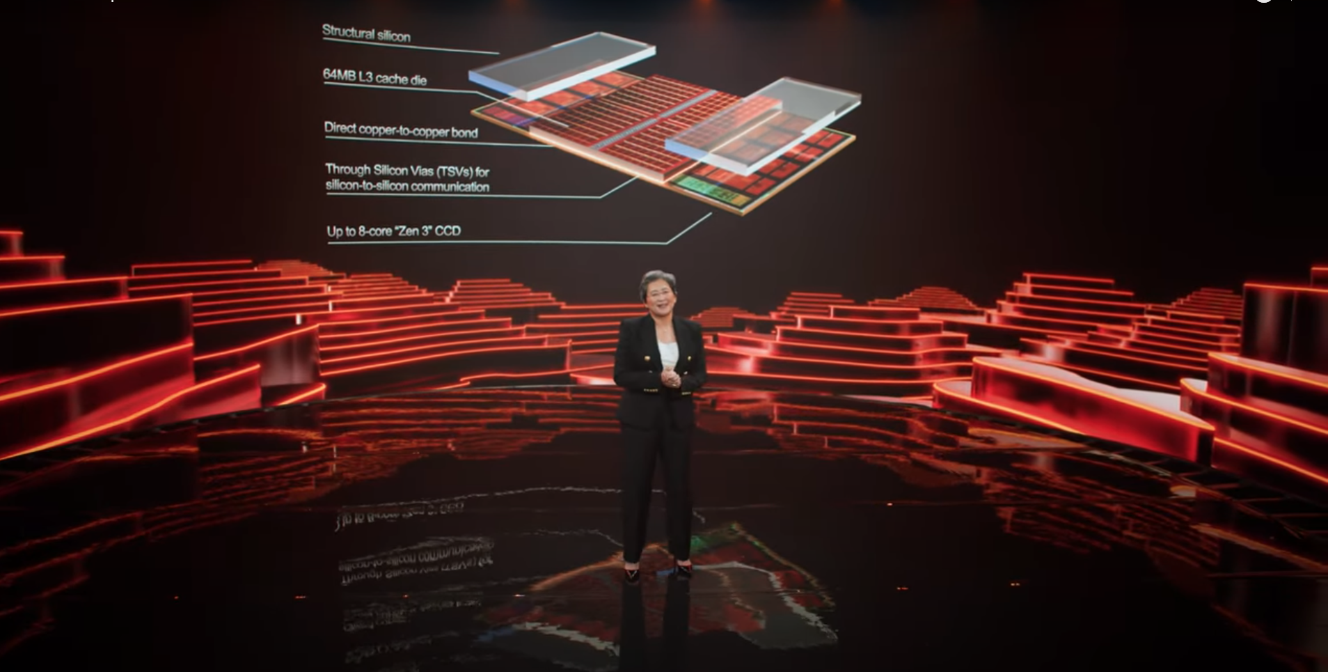
It is... the only caveat is that both chips were locked at 4ghz - so the performance numbers for the stock chip were well below where they should be. I'm guessing this was done due to the new part being an engineering sample, still I'd like to reserve judgement on the real impact of the extra cache until we see retail parts running at full clocks. It's possible the new chip may need to drop clocks a little as a result of the additional thermal overhead of the cache chip for example, which may negate the gains. It's also possible the boost doesn't scale linearly at higher clocks, or the games used here are heavily cherry picked.

That said, a very large cache like this is going to benefit many productivity workloads (arguably more than low res gaming). so I'm sure the addition will be a win overall.
 

hushnecampus

Reputable
Sep 16, 2020
56
20
4,535
I think this wound only happen with very specialized PCBs (and CPUs) where the CPU is soldered to the board. Making a CPU removable necessitates (at least currently) having the CPU too far off the PCB to make cooling it from the underside practical.

...but I still won't call you crazy. ;)
I’m not sure even soldering it to the MB would make cooling from below feasible, but if it did I’ll be happy to buy CPUs soldered to MBs. I generally update my MB the same time I update my CPU anyway, to it would have no downside as far as I’m concerned.
 

hushnecampus

Reputable
Sep 16, 2020
56
20
4,535
Could this tech have any relevance in GPUs, by the way? To be honest I’d be more excited about seeing stronger competition there.
 
D

Deleted member 2783327

Guest
All I want for Christmas, since Intel has dumped HEDT (at least for the new coupleof years), is an AMD CPU with at least 28 PCIe lanes :)
 

InvalidError

Titan
Moderator
So basically they've been starving the logic cores this whole time because they designed the chip with too little cache.
The problem with cache is that it consumes a huge amount of die space: the 32MB of L3$ in Zen 2/3 CCDs takes as much space as all of the CCD's cores combined. Doubling the total die area dedicated to cores+cache for 15% more performance isn't particularly space-efficient.
 

jkflipflop98

Distinguished
Do you have any idea how expensive cache is?! These are going to be anything BUT competitive for gamers, although against AL extra cores aren't cheap either so we will have to wait and see.

Especially since the cache only helps 15% in benches it will be next to unnoticeable in normal gameplay/ games that don't come with a bench.

Cache is actually cheap. RAM is the easiest thing to make on a node like this - and in fact most places produce SRAM as the engineering vehicle with which to qualify a new process. It's literally just a giant "array" of transistors that are exactly identical to each other like a massive farm field. Then there's a "periphery" around the (you guessed it) periphery that controls all those transistors.
 

InvalidError

Titan
Moderator
Cache is actually cheap. RAM is the easiest thing to make on a node like this
SRAM may be technically simpler to make but it has ~1/6th the density of DRAM for single-ported SRAM. However, it is common for SRAM to have 2-4 total read+write ports, so you have to duplicate the entire address decoding and data RW matrix a couple of times, making the density much worse.
 

hushnecampus

Reputable
Sep 16, 2020
56
20
4,535
The problem with cache is that it consumes a huge amount of die space: the 32MB of L3$ in Zen 2/3 CCDs takes as much space as all of the CCD's cores combined. Doubling the total die area dedicated to cores+cache for 15% more performance isn't particularly space-efficient.
Does that mean they could instead use this technology to fit the same amount of memory in a much smaller space (instead of more memory in the same space)? If so what would that enable - more cores?
 
The instruction set is likely the same, just optimized for lower power and smaller die size: you can do AVX512 on a quarter-width ALU, you just need to break it down into four extra steps.

As for it being "only relevant for laptops", I have 3100+ threads on my desktop and I'm pretty sure 3050+ of them would be perfectly fine running on low-power cores instead of making a core turbo to 4.2GHz for 10 microseconds a couple of times each second for a combined total of 5% core activity. It would probably reduce my PC's baseline power draw measured at the wall by 5-10W. While this may not sound like much, you need to keep in mind that we're also at a point where regulations are forcing the migration to 12VO to save ~10W per system.

Well part of it is they aren't HT. But lack of efficient MIMD instructions or branch predictors will affect time sensitive task. This includes rendering, cad/cam, encoding/decoding,ai training loads, and most important to us: Highly threaded video games.
 

InvalidError

Titan
Moderator
Does that mean they could instead use this technology to fit the same amount of memory in a much smaller space (instead of more memory in the same space)? If so what would that enable - more cores?
It is roughly the same total amount of die area, just stacked vertically instead of planar... and heat from CPU cores located under cache dies has to travel through cache dies to get to the IHS and HSF, so you get hotter cores. The L3 cache on the base die is practically required just to space the cores out enough to keep heat output manageable.

Well part of it is they aren't HT. But lack of efficient MIMD instructions or branch predictors will affect time sensitive task. This includes rendering, cad/cam, encoding/decoding,ai training loads, and most important to us: Highly threaded video games.
You don't need a PFLOP die to handle things like object garbage collection, network connectivity, user input, audio mixing, assets management, etc. Games have no shortage of stuff that could make use of low-power cores on top of all of the other background stuff happening in the OS. Interrupt routines and other kernel/driver-level stuff doesn't do much heavy processing, that is generally left to the user-land part of the various APIs.
 

Fdchdfa

Commendable
Apr 20, 2021
5
0
1,510
With one extra layer of silicon and interconnects between the CCD and IHS, thermals are almost certain to be a little more challenging.

As for cooling the bottom of the socket, I wouldn't expect too much out of that since heat has to go through the bed-of-pins down to the motherboard, through layers and whatever may be on the back. The thermal resistance from the die, through the CPU substrate and everything else to the back of the motherboard will be horrible. The most heatsinking I could imagine making sense there would be upgrading the mounting backplate to a small heatsink mainly to help cool the Vcore power and ground planes so they don't contribute to CPU temperature and maybe the socket just a little bit.


Woah I can't believe I have to explain this(I thought this is common knowledge) CPUs are flip chip, they flipped the chip before soldering onto the substrate, the cache chiplet is towards the side that is soldered onto the substrate, the bulk of the heat generating compute elements like the cores are not obstructed in any way whatsoever to the heatspreader, it's still a mass of bulk silicon, damn....... yeah that's right, heat has to go travel through bulk silicon before being dissipated via the heatspreader, it's why Intel performs die thinning for comet lake, to reduce the height of the bulk silicon so that heat can travel through a shorter distance through the bulk silicon to reach the heatspreader, improving heat transfer. Derbaur has some video showing this clearly
View: https://youtu.be/WOZqoTuAGKY?t=347


Cache produce little heat compared to the cores just take a look at this image the cache blocks are colder than the cores, that too is probably gets heated up by the cores nearby. The Cache chiplet gets cooled by the heatsoak of the connection pins on the substrate, while simultaneously pulling heat from the cache in the CPU chiplet since AMD is using copper connections, then the cores get cooled as usual. So all in all cooling this shouldn't be that different compared to cooling a standard zen3 CPU
 
Last edited:

Fdchdfa

Commendable
Apr 20, 2021
5
0
1,510
It is roughly the same total amount of die area, just stacked vertically instead of planar... and heat from CPU cores located under cache dies has to travel through cache dies to get to the IHS and HSF, so you get hotter cores. The L3 cache on the base die is practically required just to space the cores out enough to keep heat output manageable.
Nooooo the L3 cache needs to be in a singular location accessible by all cores in a somewhat equal latency/access time, if you split the L3 into multiple block at different location then there would be performance consequences, that is why they place the L3$ in the middle, since if you place them towards the side like Intel does for their desktop CPU, they you will end up with a very long CPU chiplet die which can't fit in the AM4 package, if you place them on both sides with the cores in the middle, then the furthest core would have significantly higher latency accessing data in the L3$ at the opposite end, so the only logical and sensible place that fit the criteria of performance/chiplet dimension/size is to place the L3$ is in the middle(Intel with their monolithic die has no choice but to split the L3$ into multiple location.) The indirect advantage of placing the L3 in the middle is spread out heat density.

Edit: Saying the main reason L3 cache is in the middle is to keep heat output manageable is false, the main reason is as stated above
 

InvalidError

Titan
Moderator
Woah I can't believe I have to explain this(I thought this is common knowledge) CPUs are flip chip, they flipped the chip before soldering onto the substrate, the cache chiplet is towards the side that is soldered onto the substrate, the bulk of the heat generating compute elements like the cores are not obstructed in any way whatsoever to the heatspreader
AMD's own video show the CCD being on the package substrate with L3 chip with flanker structural silicon and then the top filler silicon for protection. On the CPU that Su showed to the press, you can even see that the cache chip is missing its structural silicon and top slab.

If you put the cache dies under the CCDs, then you have to add a crap-ton of power and ground vias through the cache die to feed 100+A to the CCD on top, along with having to pass through the IF connection. That will ruin your cache's density. The increased electrical resistance through the SRAM won't be any good for energy efficiency and Vcore noise filtering either.
 

Fdchdfa

Commendable
Apr 20, 2021
5
0
1,510
AMD's own video show the CCD being on the package substrate with L3 chip with flanker structural silicon and then the top filler silicon for protection. On the CPU that Su showed to the press, you can even see that the cache chip is missing its structural silicon and top slab.

If you put the cache dies under the CCDs, then you have to add a crap-ton of power and ground vias through the cache die to feed 100+A to the CCD on top, along with having to pass through the IF connection. That will ruin your cache's density. The increased electrical resistance through the SRAM won't be any good for energy efficiency and Vcore noise filtering either.
So you are telling me that the cache is on top of the CCD Flip chip, so AMD would need to do the following
  1. Perform Die thinning down to a few micrometer just above the transistor layer
  2. Then tunnel through the transistor level with wires to the backside of the CCD flip chip for the cache to attach to
  3. Attach the cache chiplet to the backside of the now wafer thin CCD and place the necessary structural silicon
  4. cap off the whole CCD with a layer of silicon?

So all of that the CCD transistor would be in the middle of the whole CCD like this - substrate->dozens of metal layers->actual transistors->Silicon+wires->Cache chiplet+structural silicon. Ok then, wonder what's the yield after performing all the above steps :)
 

everettfsargent

Honorable
Oct 13, 2017
130
35
10,610
This might help ...
3d-chiplet-diagram.png

I have no idea what all the so-called structural silicon might be doped with to improve thermals. I also think the z-axis (vertical) is not to scale but expanded by some multiple of the horizontal dimensions.
 
Intel's heterogeneous cores arrangement is because it cannot do 16 high-performance cores on 10nm within a reasonable TDP. AMD is planning to do heterogeneous cores too with Zen 4D as the power-efficient cores to go along Zen 5.
Even if that would be the easiest thing for intel to do...why would they sell one 16core CPU for $500 if they could sell two 8core CPUs for $500 each, and the do can sell 8core CPUs for $500.
Selling laptop level performance for desktop prices is just good business.

Also the biggest client for intel CPUs are businesses that buy hundreds if not thousands of office PCs, if intel can lower the power draw at idle by even 10% by using laptop CPUs at idle while not loosing any multithreading performance, that alone would be a huge selling point for large customers.
 

TheJoker2020

Commendable
Oct 13, 2020
219
64
1,690
What's very curious and IMPORTANT to note here is they locked the processor at 4GHz. We all know the 5900X can run at considerably higher speeds here.

10:1 They are thermal throttling. Note the lack of thermals.

As this is essentially a demonstration product that doesn't even have a name and may not even be released on the AM4 platform, there may very well be thermal / power issues, which of course AMD would not mention at this stage.

As for "why 4GHz", perhaps this is the realistic limit of this demonstrator at the moment, or perhaps this is a simple and round number, and the CPU's were both locked to show the performance difference of the cache alone.

At this point we are merely speculating.
 

Findecanor

Distinguished
Apr 7, 2015
231
131
18,760
The speed of light "limit" only applies to a passive wire, it goes out the window once it hits logic which is much slower.
I got the speed-of-light argument from a talk by Ivan Goddard at Mill Computing, as explanation to why they divided the Mill CPU architecture's (somewhat VLIW-like) instruction stream into two: to be able to divide their instruction cache into two, with double the size as otherwise with the same latency.

Anyway, all latencies add up.
 

Findecanor

Distinguished
Apr 7, 2015
231
131
18,760
Keep in mind (Apple M1) can only support a maximum of 8GB shared memory for the entire system.
8GB is the lowest tier M1 Mac. The next one has 16 GB, and there are memory chips in the same series that Apple could have used to support 32 GB (but they didn't).

Maybe the M2 will be better, but at the end of the day M1 is still just a souped-up phone processor that has been overhyped by Apple's marketing empire.
A M1 core is a monster: wider than Intel or AMD cores, with a large reorder buffer. It is also not hampered by the limitations of the x86 instruction set, which makes it easier to decode for better IPC.

Also, the ARM instruction set simply was never designed to be good at a typical High-End Workstation/Server workload (ie tasks that benefit from an expanded instruction set / AVX), which is where the real money is at for AMD and Intel - and the customers most likely to need a giant cache.
The only advantage that AVX/AVX2 has over ARMv8-A64 is vector length. Other than that, A64 is a more modern vector ISA that was designed well from the ground up and is more complete than AVX2 and thus easier for compilers to vectorise to.
But that was before SVE, which is extended and mandatory in ARMv9 as SVE2. To match SVE on Intel, you'd need AVX-512 which isn't even a fixed ISA but for which compilers would have to produce code for specific processor types.
 

hannibal

Distinguished
The new info sirompi amd says that the v-cache is above the normal cache and on the top of cpu part there is material that is good at conducting heat, so heat output should not be very different between normal zen3 and zen3 with V-cache.
Stacking cache above the cpu die is not cheap, so these most likely will. One above normal zen3 in price. That info is not confirmed. Just based on info about the cost of making stacked cache.
 

aldaia

Distinguished
Oct 22, 2010
533
18
18,995
The SRAM itself uses almost no power. It is the tagRAM (the bit responsible for keeping track of what cache line is caching which memory chunk) that uses tons of power doing the lookups and if you are going to make the L3$ 6X as large, you can mitigate tagRAM power and latency by making each cache line 2-8X as big. With such a large cache, you should also be able to afford reducing the way-ness and associativeness of each L3$ block to simplify the tagRAM without hurting the hit rate much.

Sorry but it seems you have a misconception here. There is no such thing as tagRAM. The Tags portion of the cache is stored using exactly the same SRAM cells as the data portion of the cache. Just a few bits (typically 15 to 30 bits) of SRAM are required to store the tag for each cache block, while the data portion is usually 64 bytes = 512 bits. Therefore, TAGS amount to a small fraction of the total SRAM used and consequently it consumes a small part of the power.
Power consumption is due to mostly two factors:
  • Leakage power which happens at the SRAM cells (even if the cache is not accessed) and is proportional to the number of cells (the bigger the cache the bigger the leakage power), hence the data part of the cache is responsible of most of the leakage power
  • Switching activity on the cache wires (wordlines and bitlines), again most of the activity is due to reading/writing data and therefore is also dominated by the data portion.
 

InvalidError

Titan
Moderator
Sorry but it seems you have a misconception here. There is no such thing as tagRAM. The Tags portion of the cache is stored using exactly the same SRAM cells as the data portion of the cache.
Looks like you have no clue what tagRAM actually does and how it is completely different from SRAM. tagRAM is content-addressable memory that stores the base address bits for a given cache line and continuously compare that address against all addresses presented to the cache to match addresses with cache lines. That is billions of comparisons per second and uses considerable active power.
 

aldaia

Distinguished
Oct 22, 2010
533
18
18,995
Looks like you have no clue what tagRAM actually does and how it is completely different from SRAM. tagRAM is content-addressable memory that stores the base address bits for a given cache line and continuously compare that address against all addresses presented to the cache to match addresses with cache lines. That is billions of comparisons per second and uses considerable active power.
I do know perfectly what CAM (Content Adressable Memory) is. But CAM is not used to implement the TAG memory in processor caches. Direct-mapped caches and set associative caches store the tags in conventional SRAM cells. Only fully associative caches require CAM, but CAM is more expensive and power hungry than SRAM, and thats why (among other reasons) nobody uses fully associative caches. All processors use either direct caches or set-associative caches.
On the other hand CAM is used in L1 TLBS, but L1 TLBS are usually very small (for instance L1 TLB in zen has only 64 entries), L2 TLBs are set associative precisely to avoid the use of CAM (Zen3 L2 DTLB is 8-way 2k entries).

Since conventional SRAM and not CAM is used, the TAG side of the cache represents a small fraction of the power consumption, specially in big caches (which is the topic here). Also its worth mentioning that the TAG memory does not store the full base address bits for a given cache line, for direct and set associative caches only some bits are required, and the bigger the cache the less bits are needed per entry (wich also contributes to reduce the area and power impact of TAGs).
 
Status
Not open for further replies.