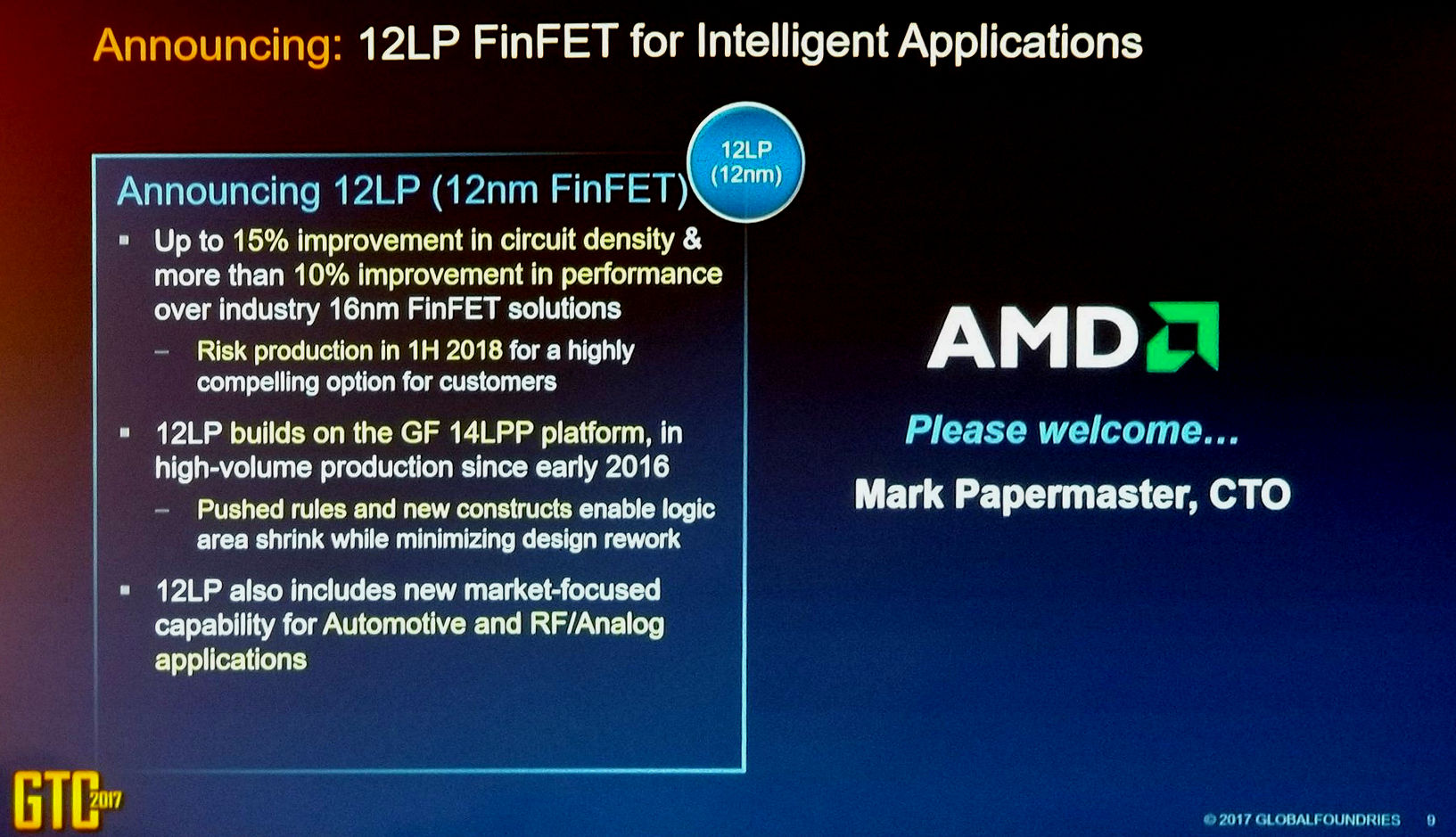
SANTA CLARA, Calif. — Globalfoundries released a flurry of announcements at an annual gathering here, including an upgraded RF process and a 12-nm FinFET node. Analysts applauded the company’s growing capabilities but said that it mainly needs to deliver in the next 12 months a competitive 7-nm process and show a volume market for fully depleted silicon-on-insulator (FD-SOI).
“I had anticipated FD-SOI revenue this quarter, but it looks like it’s a little delayed … if it slips to Q4, that’s OK, but if it runs well into 2018, it could indicate a problem getting customers to adopt a technology that may have been overhyped,” said Len Jelinek, chief fab analyst for IHS Markit. “They have big plans for that technology in their Dresden and China fabs.”
“I’m waiting to see if they hit their plans for execution on 7 nm. That’s the first leading-edge process they are developing on their own,” said Nathan Brookwood of market watcher Insight64, noting that the company licensed its 14-nm process from Samsung.
Globalfoundries’ chief technologist, Gary Patton, said that those are, indeed, his two top priorities.
“We are very focused on our [FD-SOI] road map, both on the technology and the enablement for its body bias capability, and as for 7 nm, it is an extreme sport with tight process windows that will benefit from EUV,” said Patton in a press Q&A.


