AMD's Future Chips & SoC's: News, Info & Rumours.

Page 28 - Seeking answers? Join the Tom's Hardware community: where nearly two million members share solutions and discuss the latest tech.
Status
Not open for further replies.
ill believe it when i see it. :)

if amd is relying on PRidge to be the only offering until zen2...which looks like at least a year away.

hope they put as much enhancement as they can into it.

coffee lake has closed the gap...still more expensive though...and ryzen has the edge(cores+low price) with 8 core until ice lake (or whatever lake) (8core) in q3/4 2018.
 
Well just look at what they achieved with a process designed to run chips at around 3ghz...

This new process is designed for speed I think we may be pleasantly surprised.

Just as we where with Ryzen in the first place :)

Edit: they got it to run 1ghz over what process in designed for... an this one is deigned for speed so 400/500 mhz may be quite a conservative estimate to be honest, hell we could be looking at double that with bit of luck and an IPC improvement !


It does not require a new set of MBs.
 
I feel like making screen shots just so we can go back to this point i'm expecting 200-300mhz boost at the max unless Amd woke up a year ago and realized coffee-lake was going to take a lot of fame away from Amd once it hits and maybe they should do more then a simple stepping.

So i'm not ruling out other improvements like a improved IMC, infinity fabric, and finer tuning for lower TDP parts which Amd already talked about. Also yes Turbo on ryzen is very terrible and can greatly be improved, also they need to make Ryzen turbo in 4 core and 2 core situations not just one core.


Trinity (2012): A10-5800K 3.8 GHz / 4.2 GHz

Richland (2013): A10-6800K 4.1 GHz / 4.4 GHz

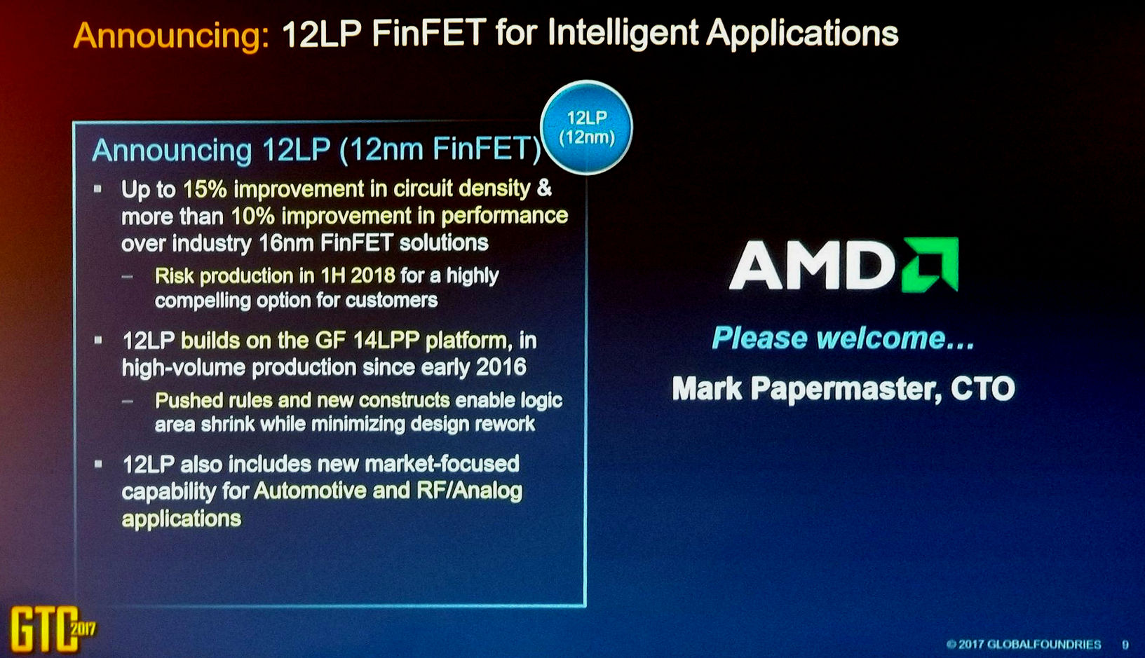
Difference in clocks was 200--300MHz and that in a process designed for speed. Pinnacle Ridge uses 12LP, which is a marketing label for 14LPP+.


I am saying that Pinnacle Ridge is a Richland-like refresh of Summit Ridge. So I am saying that they are different chips.

Bulldozer, Piledriver, Steamroller, and Excavator are all 15h family, but each is a different microarchitecture. Bulldozer is a microarchitecture. Piledriver is another microarchitecture. Steamroller is another microarchitecture, and Excavator is another microarchitecture.

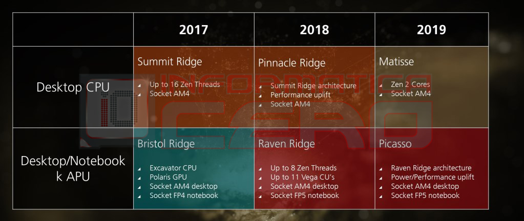
Pinnacle Ridge uses the same microarchitecture than Summit Ridge. Pinnacle Ridge uses the same Zen cores than Summit Ridge. This is on all the slides both public and leaked I repeat the 2017--2019 roadmap slide once again

AMD-Matisse-Picasso.jpg


So Pinnacle Ridge comes with higher clocks, but there is no improved scheduling; no improved branch prediction, no new instructions set support/optimization; no critical path optimizations, because it uses the same microarchitecture than Summit Ridge.

I expect improved IMC and improved inter-CCX communication from higher stock clocks. AMD also could improve the SoC with better power management or some other extra, but the microachitecture is the same than in Summit Ridge, as clearly stated in all slides.

There is no change in the microarchitecture until 2019.


Glofo is using TSMC as baseline for the marketing claims.

The 1800X has an average overclock of 4050MHz. Some chips can hit 4.2GHz whereas others cannot get 4.0GHz


I think it could be based on the high performance samsung node which uses smaller higher quality transisters an is built for speed...


Richland was Piledriver...

You REALLY need to figure out what constitutes a uarch. 15h is the uarch family. Every CPU with in that family uses the same uarch family, but EVERY base layer stepping of every CPU is a new uarch unto itself by the strictest of terms. Within the same uarch family you can have a LOT of changes, pipeline reassignments, cache size changes, etc... but a SINGLE functional change makes a new uarch.

Basically - you are saying Pinnacle Ridge will be ZP-B3. I am saying it will be ZP-C0. A new stepping - and technically a new uarch within the 17h uarch family.

Also that slide is definitely fake - stop using it. It has numerous errors.

Zen 2 is a larger change - it might include a larger/wider FPU, different pipeline layouts, different front-end, etc... 'Zen' is the CCX itself, also, and not anything else associated with it, just an FYI.


I said in this former post in this same page that Trinity and Richland used the same Piledriver microarchitecture. So there is no need to say me that "Richland was Piledriver"; I know.

I am not saying that Pinnacle Ridge is ZP-B3. I don't know the steeping that AMD will use (in fact no one knows stepping at this time, not even AMD engineers know), What I am saying is that Pinnacle Ridge uses the same microarchitecture than Summit Ridge: the Zen microarchitecture.

Also AMD has a good track record of releasing slides with marketing gibberish, typos, and obvious mistakes. Or did us forget that typo in giant font during Zen presentation?

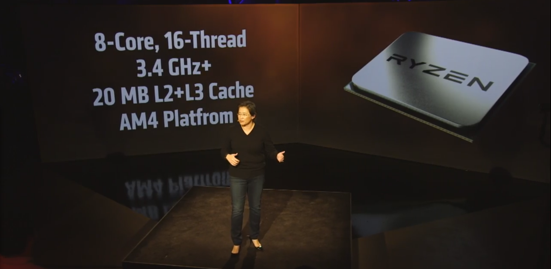
AMD-Ryzen-especificaciones.png


And yet you said this: "I am saying that Pinnacle Ridge is a Richland-like refresh of Summit Ridge." while also saying that Pinnacle Ridge isn't like the Bulldozer to Piledriver refresh. Richland WAS Piledriver, but on a different CPU.

Either Pinnacle Ridge is a new uarch or it's EXACTLY Summit Ridge. In which case AMD has gone crazy because Summit Ridge has a LOT of little problems that can be easily resolved... and resolving those issues is the same thing as what they did going from Bulldozer to Piledriver.

Let m explain how this works:

AMD consists of numerous teams, each working on a specific piece of technology we call IP (intellectual property) or "IP blocks." They do this CONTINUALLY until reassigned or they accomplish their ultimate goal, development doesn't stop and start with the generations of product we see released.

When a new CPU or stepping is released another teams takes snapshots of all progress in the 'stable' versions of the various IP blocks to implement the revised product or update an existing product. In this case, they are updating Zepplin - the dual CCX design used in Ryzen. When they do public releases they give these snapshots names like "Summit Ridge" or "Pinnacle Ridge." Each taped out update to Zepplin increments a Zepplin versioning system (which we call CPU steppings).

If AMD makes ANY changes to Summit Ridge, it should be just as grandiose as the changes made between Bulldozer and Piledriver as the same amount of time went by between tapeouts. They may not have the same net end effect (+400MHz, better efficiency, +9% IPC), but they will be on the same scale.

And, the big topper, is that AMD is moving to a new (ish) process. This involves fully rebuilding the process-specific datasets from the Zepplin master design. Once you have to do that, it's pretty dumb to not use the newest stable versions of the IP blocks as that's the easy part. Pull the schematics for the latest stable IF DDR4 IMC and plop it in place of the existing one - solve any conflicts of routing (if there are any) - a good day's work. Pull the schematics for the finalized core improvements and plop them in place of the existing core locations - solve any conflicts of routing (if there are any)... etc... People doing a process that takes a year or more won't worry about the two weeks it takes to refresh the design fully.

And, BTW, that slide is fake not just because of the typo (despite it being horribly obvious) but because of its factual errors AND improper use of terminology combined with the typo. "Pinnacle Ridge" using "Summit Ridge architecture" is a nonsensical statement. It uses "Zen" cores and is a new member of the 17h uarch. Or it's just Summit Ridge.


Exactly. Both Pinnacle Ridge and Summit Ridge use the same Zen microarchitecture. Both Trinity and Richland used the same Piledriver microarchitecutre. But Bulldozer and Piledriver are two microarchitectures.


No. Pinnacle Ridge and Summit Ridge are chip codenames, not microarchitectures.

Pinnacle Ridge and Summit Ridge are two different chips that use the same microarchitecture: Zen.


.............take the example of steppings....i think the point here is: will Pinnacle Ridge be Identical to Summit Ridge chip in design? or will it have some design improvements.?

i also doubt that it will just be an identical photocopy just using a different process. (at least i can hope there may be a few refinements...)


The only way AMD would be stupid enough to do that is if they knew, a 18 months ago, that they were going to see HUGE frequency improvements with Pinnacle Ridge and that they could get to market sooner by not messing with the uarch AT ALL.

But once they change ANYTHING functional, it becomes a new uarch by definition. They can correct critical path issues, fix microcode errors, improve the IMC, but that's about it... but that's the level of changes Piledriver saw over Bulldozer - plus the clock mesh and one enlarged buffer.

Richland, BTW, was just an APU chip name based on Piledriver. It wasn't a refresh or an update of Piledriver's uarch.

As such, you ARE saying that Summit Ridge **IS** Pinnacle Ridge... which it isn't.
 
I have a question for all. So the Zen is a good product and all yes however when it comes to AVX set, they do not support AVX512. So why they do not implement it to their CPU's. Because of licensing issues, die size, energy, cost? Can you enlighten me on this subject please.


Simple answer: it's a box they decided not to tick.

Complex answer: if they were to include AVX512, they would be adding a lot of extra transistors into their design that might not be well suited to their intended markets (initially). Intel and AMD have a cross licence agreement that allows AMD to implement most (if not all?) X86 extensions Intel has into their designs, so them not including it now is not technical (although I'm pretty sure one specific individual will argue that it is, alleging incompetence of sorts).

Cheers!


I was told the reasons were far more simple than any of that:


  • AVX512 isn't useful 95% of the time.
    AVX512 has almost no traction and is unlikely to gain much/any for years to come.
    AVX512 was Intel's way of trying to undermine the GPU compute momentum - which goes against AMD plans.
    AVX512 is really only included on *some* Intel CPUs so developers can test it for use with Intel's accelerators.

With all that, there's really no reason for AMD to support it. And, of course, the hardware requirements are quite serious, so there's a lot of work that would need to be done to support it.


Actually is really useful, It has been called a "Hidden Gem” in Intel Xeon Scalable Processors. Intel's AVX-512 is a set of new CPU instructions developed by Intel that impacts compute, storage, and network functions. I know that this is a lot to read but is the only way to actually understand the full potential of AVX-512 and how it actually improves computing.

These new set of instructions where first engineered to work with the Monstrous Intel Xeon Scalable Processors, and of course is builded into SkyLake-X.
https://ark.intel.com/products/120501/Intel-Xeon-Platinum-8160-Processor-33M-Cache-2_10-GHz

This acceleration has a number of use cases:

63 times faster high-performance computing
2 times faster AI/deep learning
1 times faster cryptographic hashing performance
2 times faster data protection

Intel AVX-512 can accelerate performance for workloads and use cases such as scientific simulations, financial analytics, artificial intelligence (AI)/deep learning, 3D modeling and analysis, image and audio/video processing, cryptography, and data compression.
Intel AVX-512 can also help data centers more efficiently use available storage resources. Simply put, it accelerates storage functions, such as deduplication, encryption, compression, and decompression. It accomplishes this by doubling the number of bits in the register from 256 to 512 (WATCH THIS VIDEO :bounce: https://www.intel.com/content/www/us/en/architecture-and-technology/avx-512-animation.html). In fact, it calculates storage functions in half the time of the previous generation.

The number 512 refers to the width, in bits, of the register file, which sets the parameters for how much data a set of instructions can operate upon at a time. Intel AVX-512 doubles the width of the register compared to its predecessor, and it also doubles the number of registers to further decrease latency.

It also contains additional optimizations to further accelerate tasks for modern workloads.

Intel AVX-512 enables twice the number of floating point operations per second (FLOPS) per clock cycle compared to its predecessor, Intel AVX2.
A single register under Intel AVX-512 can hold up to eight double-precision or 16 single-precision floating-point numbers. Or in other words,

Intel AVX-512 enables processing of twice the number of data elements that Intel AVX or Intel AVX2 can process with a single instruction, and four times that of Streaming SIMD Extensions (SSE)

Intel's AVX-512 offers a level of compatibility with AVX that is stronger than prior transitions to new widths for SIMD operations.

Unlike SSE and AVX that cannot be mixed without performance penalties, the mixing of AVX and Intel AVX-512 instructions is supported without penalty. AVX registers YMM0–YMM15 map into the Intel AVX-512 registers ZMM0–ZMM15, very much like SSE registers map into AVX registers. Therefore, in processors with Intel AVX-512 support, AVX and AVX2 instructions operate on the lower 128 or 256 bits of the first 16 ZMM registers.

Intel AVX-512 support

Release of detailed information on these additional Intel AVX-512 instructions helps enable support in tools, applications and operating systems by the time products appear. Intel is working with open source projects, application providers and tool vendors to help incorporate support. The Intel compilers, libraries, and analysis tools have strong support for Intel AVX-512 today, and updates planned (since) November 2014 will provide support for these additional instructions as well.

https://www.hpcwire.com/2017/06/29/reinders-avx-512-may-hidden-gem-intel-xeon-scalable-processors/

https://www.anandtech.com/show/11550/the-intel-skylakex-review-core-i9-7900x-i7-7820x-and-i7-7800x-tested/3

https://software.intel.com/en-us/blogs/2013/avx-512-instructions

https://software.intel.com/en-us/forums/intel-isa-extensions/topic/737959

http://www.prowesscorp.com/what-is-intel-avx-512-and-why-does-it-matter/
 
AVX-512 or all AVX-extensions of x86 basically have one purpose: process SIMD workloads as fast as possible. Guess what kind of processor is even better at that: GPUs.

However AVX has three major advantages over GPUs:

1. Unlocked DP and higher - most GPUs can only compute single precision or less, double precision comes at a heavy speed penality for most chips. (1:4 all the way to 1:32)

2. Ease of programming - if your compiler supports auto vectorization and you got good code structure, you might not even need to do anything for vector extensions to accelerate your workload. And even explicit instructions are fairly easy to use compared to OpenCL, CUDA or other libaries. New extensions still require a recompile and you might not get that for already released software.

3. Way, way better latency. But this only matters if you have a lot of switching between large amounts of numbers to crunch and complex and/or inherently serial operations. Past a certain point of data amount, for the fastest processing time, throughput becomes more important than latency.

AMD tried to tackle all this three challenges with an open hard- and software standard which development started all the way back when AMD aquired ATI. Some of you may hare heard HSA? Also, at least Bristol Ridge seems to support full DP capability for the GPU part. (2:1)
 
Still AVX 512 is only used in like 5% of applications it does need to be added to Ryzen but maybe once they get to 7nm i personally don't think its worth the extra power consumption and heat loads for a small minority currently. I mean the 1950x would cost a bit more and use a bit more power consumption if it did have AVX 512 support.


I should have been more clear: **hardware** AVX512 is not important. Supporting the instruction set and its features don't require a full width hardware (FPU, registers, etc..), but ganging resources together (for virtualized 512-bit registers and so on) works well enough. Ryzen barely suffers from doing this with AVX256 - and it could very well get away with using the same FPU and just taking even longer to execute for AVX512 - definitely would save on power.
 
SSE single precision floating point multiplications could be done twice a cycle in Haswell and Broadwell, and only once per cycle in Ivy and Sandy. They also can retire the 256 bit, 8-wide multiplications once per cycle using AVX.
If the same silicon is used for both Xeon and consumer processors, I think it's likely that the consumer ones will gain more IPC there even if they have the 512-bit instructions disabled, simply because there would be more floating point units available.


Those aren't my words. I have stated exactly the opposite than what you attribute to me. My words:


Status
Not open for further replies.