News Intel's 18A and TSMC's N2 process nodes compared: Intel is faster, but TSMC is denser

Again Apples and Oranges.
Comparing 2 chip design technologies is not as simple as which is better.

You need to compare same density against power use and termal generation. On the TSMC specs for each of the production densities that they sport, they show a graph that indicates that chips can be tailored for more performance or less power consumption.

So without knowing exactly how each chip is designed with each technology, the only thing that you can do is measure the outcomes (performance vs power consumption).

Smaller transistors tend to reduce the power consumption by itself (less material = less electrons needed to flip states = less power consumption), but as the chips are also designed with higher and higher frequencies, that economy just vanishes, and you get an higher thermal output.

So i will wait for the chips comparisons by themselves, as that is a more robust way to ascertain which is which. And is the only way that matters because those chips are the ones in the market for people to buy (not a webpage with a PR announcement).

This year is shaping to be great for product comparisons with so many new tech hitting the shelves.
 
  • Like
Reactions: bolweval and Peksha
The article said:
Intel's 18A is set to enter mass production in mid-2025 when Intel begins production of its Core Ultra 3-series ‘Panther Lake' processors, which will be available later this year. By contrast, TSMC's N2 is slated for high-volume manufacturing in late 2025, and the first products produced on this node will not be available until mid-2026 at the earliest, with mass-market products expected in Fall 2026. Samsung does not disclose when exactly its SF2 enters HVM, only stating '2025,' which could mean any time from Q1 to Q4 this year.
Intel already delayed Clearwater Forest until "1H 2026", which suggests they're facing challenges in meeting their schedule. It might turn out that TSMC's N2 isn't too far behind in ramping, compared to Intel. Between the two, I have more faith in TSMC for fulfilling their promises and holding to their schedule.

As for the nodes, Intel 18A might be technically more advanced, but TSMC has been so good at executing that I fully expect it to be competitive. It will be interesting to watch.

Also, I'm hoping that "3 nm"-class nodes ceasing to be the cutting edge will enable their use in more GPUs and client CPUs.
 
I am so excited to see these advancements across the industry. High hopes for some super processing.
I'm excited, but within limits. Let's not forget how underwhelming Arrow Lake was, in spite of advancing by 2 major nodes! Yet, it clocked lower than Raptor Lake and sometimes performed worse, while using almost as much power. I get that some of its performance problems were due to the chiplet architecture, but it was still a real head scratcher!

Zen 5 was a little less surprising, given that it stayed on pretty much the same node as Zen 4, but still a little surprising, given the move from a bleeding edge 5 nm node to a mature, optimized one.

So, I'm a little concerned that these smaller nodes just aren't going to support the kind of clock speeds we've become accustomed to, and IPC gains aren't the easiest way to increase performance.
What do you mean? Are these smaller nodes slower (clock wise)? Why would they?
 
Intel already delayed Clearwater Forest until "1H 2026", which suggests they're facing challenges in meeting their schedule. It might turn out that TSMC's N2 isn't too far behind in ramping, compared to Intel. Between the two, I have more faith in TSMC for fulfilling their promises and holding to their schedule.

As for the nodes, Intel 18A might be technically more advanced, but TSMC has been so good at executing that I fully expect it to be competitive. It will be interesting to watch.

Also, I'm hoping that "3 nm"-class nodes ceasing to be the cutting edge will enable their use in more GPUs and client CPUs.
It’s so crazy that Apple is the only company that sells consumers leading edge chips now.
 
What do you mean? Are these smaller nodes slower (clock wise)? Why would they?
Realistically they can’t say until they’re making production chips. Zen4 turned out to be able clock a fair bit better than originally expected because n5 just clocked MUCH higher than n7. That’s a large part of the reason that while AMD played down Zen4 and built up Zen5, Zen4 ended up being a much larger performance jump even though zen5 was a MUCH larger change in architecture.
 
Again Apples and Oranges.
Comparing 2 chip design technologies is not as simple as which is better.

You need to compare same density against power use and termal generation. On the TSMC specs for each of the production densities that they sport, they show a graph that indicates that chips can be tailored for more performance or less power consumption.

So without knowing exactly how each chip is designed with each technology, the only thing that you can do is measure the outcomes (performance vs power consumption).

Smaller transistors tend to reduce the power consumption by itself (less material = less electrons needed to flip states = less power consumption), but as the chips are also designed with higher and higher frequencies, that economy just vanishes, and you get an higher thermal output.

So i will wait for the chips comparisons by themselves, as that is a more robust way to ascertain which is which. And is the only way that matters because those chips are the ones in the market for people to buy (not a webpage with a PR announcement).

This year is shaping to be great for product comparisons with so many new tech hitting the shelves.
Lots of new tech promised but delivery is something else. The main thing is competition like with all monopolies on leading edge tech TSMC has pulled away and Samsung is in the race but Intel has lagged not that they have done a good job of selling their prowess as an independent Fab, but if they were able to do so this may help the inevitable march towards increased chip supply constraint.
 
No. Everywhere I've seen, people seem to believe it's just N3B (i.e. the original N3 node). Intel, themselves, has never exactly said.
Huh. Seems like this changes every time I look it up. This says that Arrow Lake is N3 and Lunar Lake N3B.
https://www.techpowerup.com/319517/...-details-n3-for-arrow-lake-n3b-for-lunar-lake

But the AnandTech link I shared doesn't acknowledge the existence of N3B. Some commenter somewhere told me N3 == N3B. I can't make sense of what's happening with N3 nodes. Except apparently Apple continues to have exclusive use of the most advanced node.
 
18A/N2 are shaping up to be the most interesting node battle we've pretty much ever seen (I hope Samsung joins the party, but they've had more issues than everyone else).

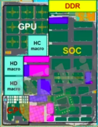
Since hitting EUV TSMC's HD cells have been extremely impressive and above everyone else. I'd be surprised if this changed at all going forward unless Intel won a big mobile production contract that demanded it. HP is another story though as they've been competitive density wise, ahead in efficiency, but behind in performance.

Right now I think the two biggest advantages TSMC has is their fab capacity and consistent execution. On paper 18A should be better for high performance, but BSPDN isn't going to be cheap and that might be the key to efficiency. No matter what though I don't think we've seen two competitive leading edge nodes before as the past was always ahead or behind.
 
Huh. Seems like this changes every time I look it up. This says that Arrow Lake is N3 and Lunar Lake N3B.
https://www.techpowerup.com/319517/...-details-n3-for-arrow-lake-n3b-for-lunar-lake

But the AnandTech link I shared doesn't acknowledge the existence of N3B. Some commenter somewhere told me N3 == N3B.
TSMC seems to have renamed N3 to N3B ...or maybe that was always its internal name and we only learned of it when they announced N3E.

I can't make sense of what's happening with N3 nodes. Except apparently Apple continues to have exclusive use of the most advanced node.
Wikichip used to have some good info on that... hey, they're back!!!


They put it on Ark when they added manufacturing nodes, and you're right it's N3B.

https://www.intel.com/content/www/u...-36m-cache-up-to-5-70-ghz/specifications.html
Wow, that's awesome! Thanks!!!
 
Realistically they can’t say until they’re making production chips. Zen4 turned out to be able clock a fair bit better than originally expected because n5 just clocked MUCH higher than n7. That’s a large part of the reason that while AMD played down Zen4 and built up Zen5, Zen4 ended up being a much larger performance jump even though zen5 was a MUCH larger change in architecture.
Zen 5 was mostly all about server. EPYC Turin saw huge gains in performance compared to Genoa. For desktop users, these changes made little difference, although Linux see's much better uplifts and Windows has sucked a lot of the life out of Zen 5.
 
Huh. Seems like this changes every time I look it up. This says that Arrow Lake is N3 and Lunar Lake N3B.
https://www.techpowerup.com/319517/...-details-n3-for-arrow-lake-n3b-for-lunar-lake

But the AnandTech link I shared doesn't acknowledge the existence of N3B. Some commenter somewhere told me N3 == N3B. I can't make sense of what's happening with N3 nodes. Except apparently Apple continues to have exclusive use of the most advanced node.
There was never N3, it always launched as N3B for whatever reason, and was widely panned as bringing the worst generational node uplift in TSMC's history. It was always amusing how Apple with their deep pockets rushed into 3nm just for bragging rights and didn't care about the higher wafer cost for minimal improvement over N4P. It was equally sad to see Intel dump 20A for Arrow Lake (at least i3/i5) and go for N3B, not N3E.

I'm excited for 18A as it also brings GaaFET and backside power delivery. If it also has the rumoured improvements to memory controller being moved back to the cpu tile and fixes latency issues (maybe ringbus changes) Panther Lake could be excellent. Lunar Lake is already a nice apu, and Panther Lake brings major improvements. In fact, Panther Lake can be made for desktop and I'd rather see that than a crappy Arrow Lake refresh which basically adds nothing but a stronger NPU.
 
  • Like
Reactions: TheSecondPower