AMD Vega MegaThread! FAQ and Resources

Page 31 - Seeking answers? Join the Tom's Hardware community: where nearly two million members share solutions and discuss the latest tech.
Status
Not open for further replies.


AMD needs feature that can be used automatically in games without any special tweak to use the said feature. async compute for example only accessible via DX12 or Vulkan. AMD not the only one have GPU utilization issue. nvidia to certain extend also face similar issue. the changes from kepler to maxwell for example one of the primary changes nvidia did to the SM layout was to increase GPU utilization (for gaming in general). but the changes that nvidia make did not need specific feature to be supported by games. hence it should benefit any games regardless of API being use.
 

goldstone77

Distinguished
Aug 22, 2012
2,245
14
19,965
What needs to be done to start a Navi thread? Or maybe a Future Radeon Graphics cards/News/Rumors?

AMD 7nm “Super Secret” Navi GPU Spotted In Driver, 2H 2018 Launch Expected
By Khalid Moammer
19 hours ago

AMD’s upcoming next generation 7nm based graphics architecture codenamed “Navi” has reportedly been spotted in Linux driver code. The all new GPU architecture is officially slated to debut next year, with all whispers indicating a debut in the latter half of the year.

Navi was peculiarly hidden behind a “Super Secret” ID. No, really, that’s what AMD’s driver whiz’s have listed it under. The code reads:
“new_chip.gfx10.mmSUPER_SECRET.enable[0:0]”

The Vega architecture is GFX9. Navi is GFX10, which is what gave this new “Super Secret” chip away.
 
AMD needs a Polaris replacement soon. I don't think they can let Navi slip to 2019, at least, not the mainstream version of it.

Was Navi going to be full stack or Polaris was going to have it's own successor that wasn't Navi?

Cheers!
 

Rogue Leader

It's a trap!
Moderator


I kind of remember reading something that Navi was going to be a new architecture and move away from GCN, so that will be the basis of new cards.

Take that for what its worth though its literally a vague memory from an older article.
 
Polaris probably will be succeeded by Vega. AMD already using some form of Vega inside their newest APU. When AMD coming up with new flagship they usually fill the lower tier with rebrand. Though i don't believe AMD will use polaris to fill the mid range in 2018 for the third time. If we follow AMD usual trend then below Navi most likely Vega 64 and 56 being rebrand into new series. If polaris did not get another rebrand (like Pitcairn) then mid range vega most likely going to fill the gap.


I recall reading that "Vega 12" would be the replacement for Polaris after the process shrink and subsequent release. It will be interesting to see how much of a difference going from 14nm to 12nm will make. I'm hoping they are taking the opportunity to do a few tweaks at the same time. Plus whatever "Vega 20" is supposed to be.

Navi only shows "Scalability and Next gen memory" from the last map they released....which should be interesting as it seems the speed of HBM2 is more a hindrance on Vega than Vega's clock rate...or so i keep reading.

Has AMD released anything further about the process shrink releases?
 

goldstone77

Distinguished
Aug 22, 2012
2,245
14
19,965
What needs to be done to start a Navi thread? Or maybe a Future Radeon Graphics cards/News/Rumors?

AMD’s Next-Generation Navi GPU Could Ship by Late 2018
By Joel Hruska on December 19, 2017 at 11:15 am

AMD’s Navi has been of interest to AMD fans since it first popped up on roadmaps, with hints of a next-generation memory subsystem and a “scalability” option that might be similar to the modular GPU designs that Nvidia is supposedly considering for its own products. First, the hints. As Hot Hardware reports, some driver notes for a Linux driver update back in July that were recently discovered reported:

[WARNING]: Should use –pci when using create_asic_from_script()
new_chip.gfx10.mmSUPER_SECRET => 0x12345670
new_chip.gfx10.mmSUPER_SECRET.enable[0:0]

GFX10 is a Navi reference, and there are plenty of other hints to ongoing Navi work at AMD, from a job opening for a senior ASIC design and layout engineer (Shanghai, China) to various statements from AMD that it’s working on 7nm ramps already (the remarks date to May of this year). A Navi tape-out now or in the next few months would clear the way for a professional product introduction late next summer or fall, with consumer cards arriving a few months later
59428_03_amds-next-gen-navi-gpu-launching-august-2018.png

As for what the GPU will be, that’s anyone’s guess. AMD and Nvidia have both made noise about scalability and building distributed GPUs, but such designs come with a lot of potential issues that need to be addressed. GPU internal bandwidth is much, much higher than what we’ve seen in multi-core CPUs interconnects — think along the lines of 300GB/s, as opposed to 30GB/s. Building an interconnect that could keep all the subdivided GPU components suitably fed would be a very careful balancing act. I’m not suggesting that NV, AMD, or both won’t build it, but it may not be an easy road to delivery.

Frankly, I’m not sure now is the right time for AMD to be clever as far as GPU design is concerned. HBM and HBM2 may have delivered some benefits to AMD’s overall power consumption profile, but the company has had to push all of its GPU designs extremely hard to match Nvidia’s performance going back as far as Hawaii in 2013. Granted, Vega doesn’t hit the 95C temperatures that Hawaii did, but AMD didn’t really deliver the performance or power consumption that people were hoping for in 2017, either. If Navi cleans up cruft in the Vega design and delivers a large performance uplift thanks to further design refinements, so much the better, even if it isn’t a brand-new architecture or major design shift compared with Vega. Either way, repeated rumors are pointing to 2H 2018 for a refresh from Team Red.


jaymc

Distinguished
Dec 7, 2007
614
9
18,985
I came across this earlier, it saying the leak is a fake ?

"We’re no masters of Linux driver code, but Phoronix are, and it turns out we were right to doubt what seemed like fake code. Not only is the code from a demo file, it’s not even for Linux drivers - it’s for AMD’s UMR, or rather, their open-source GPU debugger software."

https://www.pcgamesn.com/amd-navi-linux-drivers


Well, I would imagine all the new games still use DX9c in essence, but are using the newer libraries in their bundles with 1 or 2 new DX12 features.

I wonder if AMD will be quick about this one. There's plenty of games out there using DX9c that are still used quite frequently.

Cheers!


What they've said so far is that they will not fix it.

But then it only affects a few older titles. Newer titles, even if they're DX9, should be okay.
 

Kulasko

Honorable
Jun 13, 2013
30
0
10,540
I read there are just some missing libaries which can be installed after the driver and probably will be included in a coming hotfix.
 

AndrewJacksonZA

Distinguished
Aug 11, 2011
574
91
19,060
They dared mess with my beloved C&C franchise, I might just jump ship to Nvidia with my next purchase. Who cares about business ethics, openness, open source support, FreeSync and GPUOpen? #CnCUberAlles #TeamGDI

:)


I thought they were? Wasn't there a tweet from a guy from AMD saying they were working on a fix for it? I will probably be what Kulasko said about including the updated libraries in the driver (if that is the problem).

Cheers!


Right now it might be a few tittles. but what about future drivers? if future driver break more DX9 games then AMD will also not going to fix those regardless the game being new or not. that actually what trigger much bigger reaction from PC community. of course after the blowback from community AMD decided to "fix" the problem.


Yes, they reversed their earlier statement (which was via the support system and less authoritative).
 

goldstone77

Distinguished
Aug 22, 2012
2,245
14
19,965
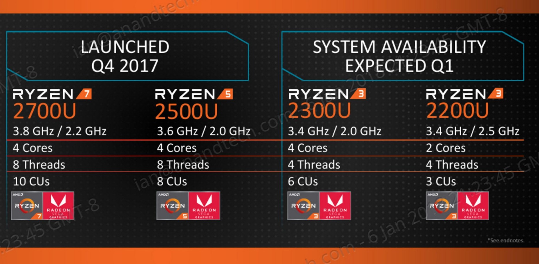
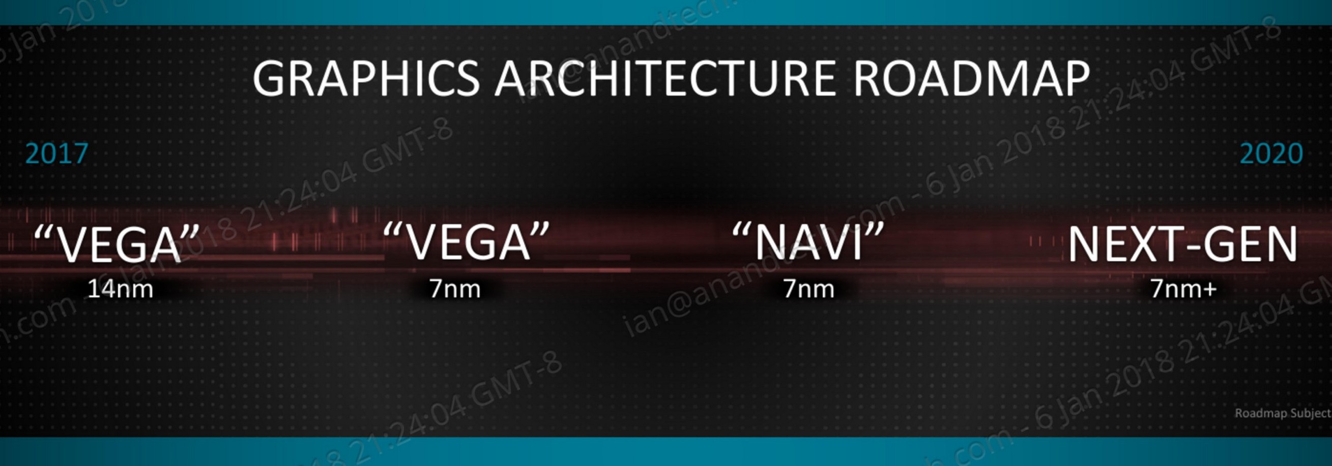
AMD Tech Day at CES: 2018 Roadmap Revealed, with Ryzen APUs, Zen+ on 12nm, Vega on 7nm
by Ian Cutress on January 8, 2018 12:01 AM EST

https://www.anandtech.com/show/12233/amd-tech-day-at-ces-2018-roadmap-revealed-with-ryzen-apus-zen-on-12nm-vega-on-7nm
roadmap2.jpg

ryzen_mobile_skus.jpg

gpu_to_2020.jpg

Also on the list is perhaps the surprise announcement of the day: AMD will be bringing Vega to 7nm, with customer sampling expected to start in 2018. This ultimately means that Vega on 7nm will hit the shelves in 2019, but there is a twist to the tale. The first products off the line will be solely for the Radeon Instinct family and machine learning. Users who want 7nm desktop-class products will have to wait a little longer, but it does give an indication of how GlobalFoundries 7nm process is coming along.
 

goldstone77

Distinguished
Aug 22, 2012
2,245
14
19,965
Samsung brands second-gen HBM2 as 'Aquabolt'
Now in mass production
By Shawn Knight on Jan 11, 2018, 12:40 PM
https://www.techspot.com/news/72712-samsung-brands-second-gen-hbm2-aquabolt.html
Samsung on Thursday announced it has started mass production of its second-generation 8GB High Bandwidth Memory-2 (HBM2). The package, dubbed Aquabolt, delivers data transfer speeds of 2.4 gigabits-per-second (Gbps) per pin which Samsung says translates into a performance boost of nearly 50 percent compared to its first-gen offering.
Samsung’s first 8GB HBM2 package offered a transfer rate of 1.6Gbps at 1.2V (and 2.0Gbps at 1.35V). Aquabolt gets the job done at 1.2V.
The new package will offer a 307 gigabytes-per-second (GBps) data bandwidth, achieving 9.6 times faster data transmission than an eight gigabit (Gb) GDDR5 chip, which provides 32GBps of bandwidth.
As Samsung highlights, using four of the new HBM2 packages in a system will enable 1.2 terabytes-per-second (TBps) of bandwidth.
Samsung notes that achieving Aquabolt’s unprecedented level of performance required the use of new technologies related to Through Silicon Via (TSV) and thermal control.
A single 8GB HBM2 package, for example, consists of eight 8Gb HBM2 dies that are vertically interconnected using over 5,000 TSVs per die. Using that many TSVs can cause collateral clock skew although Samsung was able to minimize the skew and boost chip performance in the process. To keep temperatures in check, Samsung increased the number of thermal bumps between the HBM2 dies and even bolstered the package’s overall physical strength by adding an additional protective layer at the bottom.
Samsung didn’t say when it would be supplying the new memory to partners although if it’s already in mass production, one can hope that partner availability won’t be too far out.

WOW, GDDR6 is only 16GBps! And up to 32GB! I wonder how fast this jumps into AMDs new design plans?
 
Status
Not open for further replies.