AMD's Future Chips & SoC's: News, Info & Rumours.

Page 39 - Seeking answers? Join the Tom's Hardware community: where nearly two million members share solutions and discuss the latest tech.
Status
Not open for further replies.


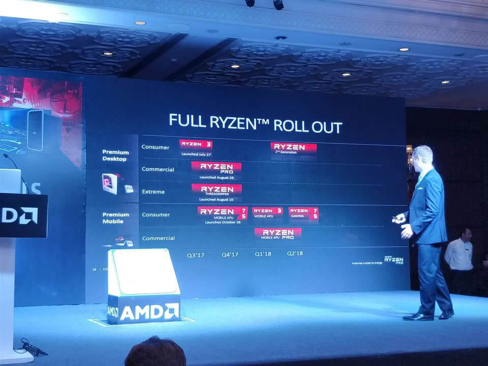
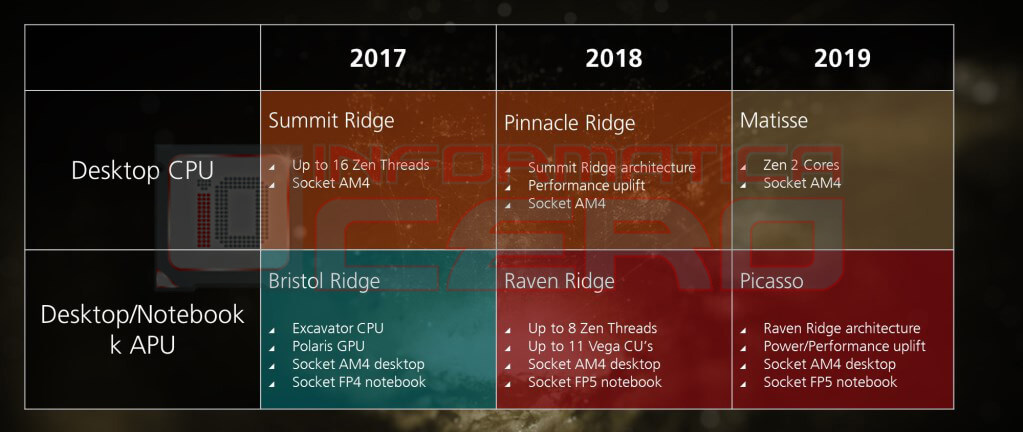
There is no 12nm node. "12LP" is a marketing name for 14nm+. There is no Zen+, as showed in the roadmaps given above.

Zen in 12LP continues being Zen. The microarchitecture is the same. That is why the AMD roadmap puts "Zen" in giant font.


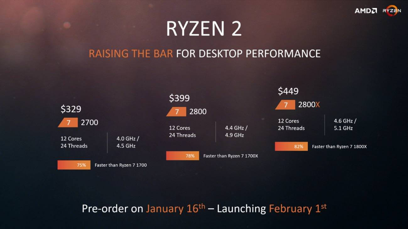
As I already said in this former post that slide is a fake. My demonstration that slide is a fake was made on day 4 and can be found here.

Besides that, the rest of Techspot article by Rob Thubron is a collection of nonsense.


You are back tracking your statements refuting your claim about AMD technical docs first paragraph... Then you make another claim about 50% more cores and 1GHz, but previously stated motherboard makers can design motherboards to handle ~whatever power draw they want. The fact that it originated on reddit via post AYYMD makes the slide questionably a fake not your contradictory statements last week.


There are absolutely no contradiction in my statements. One thing is the spec, another is overclocking beyond the spec. AMD cannot do a chip advertised for an AM4 platform that violates the AM4 spec they designed. AMD couldn't sell a AM4 chip that would work only in some few AM4 mobos. And even those high-performance mobos that could handle the loads would be a source of unending problems. Forcing mobos to always run beyond the spec would generate all kind of legal conflicts for AMD not only with final users, but with motherboard makers.

So with a five minute exercise, I knew the slide was fake.
 
of course the slide is a fake.

the specs maybe closer on a 7nm process. imo. enabling higher clocks. and more cores.

4.5 ish GHz on their improved 14nm process. maybe. actual performance increase 5-10%
dont expect miracles until 7nm and a more revised design.

but it all comes down to how good the '12nm' design is. and whether it can compete with intel's 14nm++
who knows? only glofo and amd..not even them until they have working samples to test :lol:


This is what took you 5 minutes and is the basis for your argument for the slide being fake... .. . . . Care to explain? AM4 has a 140W+ TDP and the 1800X is a 8 core with base clock 3.6GHz and TDP of 95W.


12LP = 14LPP+

Fin, Gate, and Interconnect Pitches are the same than for 14LPP. SRAM density is not public, but apparently 12LP uses higher-performance libraries, which will reduce the density. No way 14LPP+ can compete with Intel 14nm++.

12LP could provide 5--10% higher clocks than 14LPP.


That is only a part of my argument. The other part is where I mention the physical impossibility of 12LP reducing this wattage by a factor of ~3x to fit within the AM4 socket spec limits.

Per spec. the "AMD socket AM4 reference limit" is 128W.

140W is the rating for some coolers.

The '95W' of the 1800X is a marketing value that doesn't correspond to the real TDP. The real TDP is higher as confirmed by reviews.


The thermal design power (TDP), sometimes called thermal design point, is the maximum amount of heat generated by a computer chip or component (often the CPU or GPU) that the cooling system in a computer is designed to dissipate under any workload.

Power consumption is not TDP. Please list the reviews stating that thermal design power was not 95W. This should be fun since there is not set standard for TDP, and it depends entirely on what the manufacturer decides constitutes a 95WTDP workload.


Power consumption is TDP. The first law of thermo states all the heat dissipated by the CPU comes from the power consumed by the socket.

Virtually any review of the 1800X reported how the real TDPs aren't those that AMD marketing claims. There is a de-facto standard for the definition of TDP and AMD did broke it, inventing a false TDP formula for RyZen to mislead people. People looking at TDP marketing value would believe that 95W RyZen is more efficient than the 140W of Broadwell-E, but in reality the '95W' dissipates about same power (~130W):

In fact, despite the 95 watt TDP, the Ryzen CPU uses about the same power as the 140 watt Broadwell-E processors.

The more complete discussion is on the Hardware.fr review:

TDP and TDP ...

Indeed with a consumption measured on the ATX12 at 128.9 watts, it is obvious that the consumption of the Ryzen 7 1800X exceeds the 95 watts announced on TDP (Thermal Design Power). Indeed even if we base on a yield of 85% in the power stage of the motherboard, we arrive at almost 110 watts. An estimate confirmed by the internal monitoring of the processor which even indicates 112 watts under x264.

At Intel, the consumption limits for the Turbo and the TDP are identical, which seems the most logical since each watts consumed by the processor is discharged in the form of heat. In very rare cases, which do not correspond to a realistic load, in particular 100% AVX load, consumption can exceed this common value even at the initial frequency. For Ryzen, AMD uses another formula:

TDP (Watts) = (tCase ° C - tAmbient ° C) / (HSF ° C / W)

The three values ​​on the right are defined in this way:

tCase ° C: maximum temperature at the junction between the die and the HIS necessary to maintain the expected level of performance.
tAmbient ° C: maximum ambient temperature of the housing needed to maintain the expected level of performance.
HSF ° C / W: Minimum thermal resistance of the cooler to maintain the expected level of performance.

For the 1800X and 1700X, these values ​​are respectively 60 ° C, 42 ° C and 0.189. For the 1700, it is 72.3 ° C, 42 ° C and 0.451. The formula gives respectively 95.23W and 64.96W.

If linking all these values ​​is logical when defining thermal specifications, AMD benefits our sense of the lack of a standard for defining what a component's TDP should be. The result of this formula is not a TDP in the usual sense of the term but the number of watts of the processor that must be dissipated (and therefore it can consume) to maintain its maximum performance under certain conditions.

What are then the TDP, in the sense of the limit of consumption and thus the maximum number of watts to be dissipated, Ryzen? AMD also communicates this value, less markedly: 128 watts for the 1800X / 1700X, and 90 watts for the 1700. These are the values ​​that are the most comparable with the TDP released by Intel.

The real TDP of the 1800X/1700X is 128W. The real TDP of the 1700 is 90W.

HFR confirmed via measurement the 128W on the 1800X. Canard confirmed the 90W for the 1700:

https://mobile.twitter.com/CPCHardware/status/843109717610287105/actions

The 1700 pulls 90W in reality. AMD bullshit its TDP.


Can you give link to the discussion on Hardware.fr? Twitter link did not work. Also, by their own admission the commenter realizes their is not standard for TDP, and is making a guess based on assumptions and making it up as he goes and omits AVX workloads from Intel chips, because he just doesn't think it's realistic. So, he is picking and choosing how he wants to come up with these numbers. How can I take anything based on his opinions seriously?
If linking all these values ​​is logical when defining thermal specifications, AMD benefits our sense of the lack of a standard for defining what a component's TDP should be.
Since safety margins and the definition of what constitutes a real application vary among manufacturers, TDP values between different manufacturers cannot be accurately compared. For example, while a processor with a TDP of 100 W will almost certainly use more power at full load than a processor with a 10 W TDP from the same manufacturer, it may or may not use more power than a processor from a different manufacturer that has a 90 W TDP. Additionally, TDPs are often specified for families of processors, with the low-end models usually using significantly less power than those at the high end of the family.

The dynamic power consumed by a switching circuit is approximately proportional to the square of the voltage:[7]

where C is capacitance, f is frequency, and V is voltage.
\

Edit: Have you ever used an Intel heatsink and fan? They don't come close to the TDP of the processor.
 
TDP means "thermal design power". It does NOT mean "maximum power that the processor can consume while in a less constrained environment". TDP means exactly "thermal power dissipation the system has to tolerate/dissipate off the processor in order for it to work properly", in which "properly" means not falling under base clock.

And this even it only for the processor, not accounting for everything else including the VRMs.
For that reason, it really doesn't make any sense at all to compare processors by TDP or compare TDP with the power draw while using better cooling and measuring before the VRMs.
 
December 13, 2017

When AMD introduced its EPYC chip line in June, the company said a portion of the line was specifically designed to re-invigorate a single socket segment in what has become an overwhelmingly two-socket landscape in the data center. Today, AMD and Baidu announced that China’s giant internet provider would offer AI, big data, and cloud computing services on EPYC-based single socket solutions.

This deal follows last week’s announcement that Microsoft Azure would offer EPYC-based instances (see HPCwire article, Azure Debuts AMD EPYC Instances for Storage Optimized Workloads). The EPYC line’s high memory bandwidth and IO capacity makes it well suited for many areas but especially for storage servers. AMD is working to ensure EPYC doesn’t become stereotyped by this perception.

“You have probably seen in the industry a fair number of single socket platforms from us but they have tended to be more on the storage optimized or GPU optimized,” said Scott Aylor, AMD corporate vice president and general manager of Enterprise Solutions. For example, HPE introduced a storage optimized server, CL3150, using a single socket EPYC design. “Given the variety of services that Baidu deploys, including storage but also others, I want people to know this is really a compute oriented platform,” said Aylor.

It’s clear AMD is targeting price-performance points that it hopes Intel will find difficult to match and that will help AMD reclaim chunks of the x86 data center market after a lengthy absence. The single socket gambit is an important part of the strategy as was made clear by Aylor at the June launch.

“We can build a no compromise one-socket offering that will allow us to cover up to 50 percent of the two-socket market that is today held by the [Intel Broadwell] E5-2650 and below.

“In our one socket offering we have come up with a clever way to maintain all of the I/O capabilities that you would get in a two socket as well as the full complement of eight memory channels. Today people buy two socket, sometimes because they need to, but more often than not because they have to. There are many examples in which I/O rich [workloads] like storage, like GPU compute, and some vertical workloads where people don’t necessarily need two sockets from a CPU performance perspective,” said Aylor.

AMD contends the EPYC processor will deliver 2.6X the I/O density than competitive solutions and enable Baidu to achieve a level of scale and efficiency unrivaled in high-performance x86. “The combination of performance from the EPYC processor cores, and compute and I/O density packaged in a single-socket configuration, provides the ideal platform for Baidu’s next generation cloud services,” according to AMD.

“By offering outstanding performance in single-processor systems, the AMD EPYC platform provides flexibility and high-performance in our datacenter, which allows Baidu to deliver more efficient services to our customers,” said Liu Chao, senior director, Baidu System Technologies Department in the official release.

Again, from the EPYC launch in June, Aylor said, “We’ve selectively optimized a couple of skews for one socket only. So these are skews that are one socket capable only.” As an example of how the one socket and two socket offerings are distinguished, he cited on package interconnect, “The infinity fabric that would normally connect the two sockets in a two socket system, we repurpose that interconnect into more I/O lanes and that’s how you have in a two socket solution 128 lanes of PCIe and in a one socket solution you still keep the same level of connectivity.”

Today’s announcement punctuates what has been a heady year for AMD. Adoption of the single socket solution by Baidu is another demonstration of market traction and according to AMD, Baidu expects to expand its use of EPYC processors across its global datacenters beginning in the first quarter of 2018.

“This announcement with Baidu and the fact that it is AI, big data, and cloud; those are all computing oriented workloads. So think about the point we raised when we first launched [which] is we now can take what has been part of the mainstream of the market and everything that historically has been the [Intel] E5-2650 and below, and really, looking at the [Skylake] Silver and Gold today from [Intel], we can really address that now with a single socket platform,” said Aylor.

It will be interesting to watch how big a swath AMD’s single socket initiative can cut in the competitive data center market. Aylor said more and more varied single socket EPYC-based offerings are coming, but didn’t specify from who or when.

Information supplied by AMD: AMD EPYCTM processor supports up to 128 PCIe Gen 3 I/O lanes (in both 1 and 2-socket configuration), versus the Intel Xeon SP Series processor supporting a maximum of 48 lanes PCIe Gen 3 per CPU, plus 20 lanes in the I/O chip (max of 68 lanes on 1 socket and 96 lanes on 2 socket). NAP-56


https://www.hpcwire.com/2017/12/13/amd-wins-another-baidu-deploy-epyc-single-socket-servers/
 
Huge AMD ‘Fenghuang APU’ with 15FF Graphics Spotted – The Ryzen APU For Desktop
By Usman Pirzada
3 hours ago

So something pretty interesting popped up on SisoftSandra database recently, a very large APU that has the branding of AMD’s next generation avian roadmap. Codenamed ‘Fenghuang’, this APU houses a very large number of CUs (28 to be exact) with roughly 1792 SPs making it one of the largest APUs we have seen so far. This appears to be the APU for Desktop that we know has been in the pipeline for quite a while now.

AMD Fenghuang to reign over all others, huge 28 CU APU for desktop spotted on SiSoft Sandra
AMD has always chosen very interesting nomenclatures for its products. While other semiconductor companies usually have systematic (and boring) nomenclatures based on an alphanumeric sequence AMD has always opted for naming its pet products after something real. The Avian nomenclature series is no different and while it starts from the 14nm process, it carries on into the 7nm node as well.
Fenghuang are mythological birds of East Asia that reign over all other birds according to wikipedia and this indicates the importance of the product to the company internally. The entry lists AMD Fenghuang as the primary platform and the CPU in question is a Ryzen part. There is a distinct possibility that we might actually be looking at an 8-core Zeppelin die based APU – something we have heard rumors of before. Before we get into more details however, this is the entry in the flesh:
AMD-Fenguang-APU-with-15FF-Graphics-Ryzen-APU-Desktop.jpg

As we can see, the SP count listed is 1792, which would make it the largest APU to date. The integrated graphics portion gives away the fact that this is an APU, not to mention the fact that the “AMD Fenghuang” platform name can be seen below as well. The core clocks of the CPU side of things are slated at around 2.4 GHz, with turbo probably being around 3 GHz. The APU has a 16 kB cache and 2GB of memory (is that HBM?).

The clock speed of the GPU is currently listed at 555 Mhz, this is almost certainly a pre-launch engineering sample number and one we expect to go much higher to 700 MHz at the very least. This would mean you are looking at a theoretical peak performance of 2.5 TFLOPs. This clock speed might seem a bit on the low side but keep in mind this is an APU and one that might actually be housing a Zeppelin die along with it so the company is playing with a very small thermal envelope here.
Now there is a bit of an oddity in this spotting, and that is the memory bus width which is listed as a tiny 32 bit. This is, frankly speaking, not possible which leads us to believe that the tool might be misreading the number due to the unique construction of the APU. It is even possible that the GPU is powered by HBM memory, which would explain the confusion faced by the tool. The memory clocks listed are 2400MHz on the tool.
 
From tom's hardware:

"And it's notable that the 95W Ryzen 7 1700X we're reviewing today uses less power under our stress test than Intel's 91W Core i7-7700K."
 
Intels definition of TDP from it's product specification:
"Thermal Design Power (TDP) represents the average power, in watts, the processor dissipates when operating at Base Frequency with all cores active under an Intel-defined, high-complexity workload."
Key points:
Average Power (not max power)
Dissipated at BASE FREQUENCY (not turbo frequency)
and the most relevant, INTEL DEFINED WORKLOAD


Note "high-complexity workload" does not include AVX!
 
Here's another "good read" from Mr Morgan over at the next platform:

"The important thing to note here is that these are not proof of concept deployments. They are not tens or even hundreds of machines used in a proof of concept, but thousands of machines that have been deployed already in 2017 at Microsoft and Baidu, and with every prospect of this growing to tens of thousands of machines in 2018 as more workloads come into play at these companies."

Check it out here: https://www.nextplatform.com/2017/12/13/two-hyperscalers-amds-epyc-six-go/
 
As part of a school thesis for research I've got to search sites with relevant information on given topic and provide them to teacher our opinion and the article. Your post helped me a lot. This is my first time see here. From the tons of comments on your articles, I guess I'm not just one having all the enjoyment right here! I just couldn't leave your website before telling you that I truly enjoyed the best high quality articles you present for your visitors? Will be returning again frequently to check up on brand new posts.

Mod removed links.
 
Quoted from the article: "Microsoft could have launched a much-improved L Series instance using Skylake Xeons and added in twice as much memory and 2.5X the storage. But the point is, Microsoft did not do that, and AMD got the business instead."

There may be many reasons for that decision, not least being vendor diversification.

I've said before an I'll say it again everybody wants AMD to succeed !

An Some poeple claimed it would never happen, design wins for Epyc. An massive ones as well... I gues they couldn't of been more wrong about that.
 
IEDM 2017: GlobalFoundries announces 7nm chipmaking process
The development of its own 7nm technology is a significant milestone for customers like AMD and IBM that need the highest performance. But GlobalFoundries has also evolved into a full-service foundry with a range of technology and products.
John Morris
By John Morris for Between the Lines | December 13, 2017 -- 18:42 GMT (10:42 PST)

iedm-gf2.jpg

iedm-gf1.jpg

n a late addition to this year's IEDM 2017 lineup, GlobalFoundries unveiled details of its 7nm process which promises a significant increase in density, performance and efficiency in comparison to the 14nm technology used to manufacture AMD processors, IBM Power server chips and other products. GlobalFoundries will start 7nm production using current lithography tools, though it plans to quickly move to next-generation EUV lithography to cut costs.

Based on GlobalFoundries latest generation of 3D or FinFET transistors, the 7LP process has a fin pitch (the distance between the conducting channels) of 30nm, gate pitch of 56nm and a minimum metal pitch of 40nm--all of which are "significantly scaled from 14nm." GlobalFoundries said it tuned the fin shape and profile for best performance, but did not provide measurements for the width or height of the fins. The smallest high-density SRAM cell measures 0.0269 square microns.

These feature sizes are similar not only to TSMC's 7nm process, but also to Intel's 10nm process, which is roughly equivalent to what the foundries refer to as 7nm. (Samsung will provide details of its 7nm process, which uses EUV from the outset, at ISSCC in early 2018.)

GlobalFoundries will offer two different flavors of 7LP. The high-density standard cell for mobile processors has two fins and is only 240nm tall translating to a 0.36x area reduction at the SoC level compared to 14nm. A separate version for high-performance servers such as IBM Power has four fins, as well as larger contacts and wires, and operates at a higher frequency.

Overall GlobalFoundries is promising a 2.8x increase in density, and either a 40 percent boost in performance or 55 percent reduction in power at the same performance. The high-performance version can deliver another 10 percent boost. Those are some impressive numbers, but it is worth underscoring here that GlobalFoundries is comparing this to its current 14nm process (licensed from Samsung) because it is skipping 10nm (though it will offer an interim 12LP process with 15 percent higher density and 10 percent better performance starting early next year). TSMC adopted a similar strategy when it unveiled a 7nm 256Mb SRAM test chip at last year's conference, comparing it to its current 16nm process rather than what it says will be a "short-lived" 10nm node.
Like Intel, GlobalFoundries will use self-aligned quad patterning (SAQP) to fabricate the fins, as well as double-patterning for metal layers, and has introduced cobalt metal contacts to reduce resistance. As a pure-play foundry, it will offer a wide range of metal stacks for different applications. The technology also supports a range of threshold voltages (the gate voltage at which the device turns on) without doping, which GlobalFoundries says improves performance and reduces variability.

GlobalFoundries plans to introduce EUV lithography in two stages. First, it will use EUV only for contacts and vias, cutting more than 10 lithography steps out of the process to reduce cost without requiring customers to redesign their chips. It will eventually use EUV for several critical layers, a step that will require a redesign but should deliver additional power, performance and area benefits.

The 7LP process will be in trial production in mid-2018, which means it will be volume production in the fab in Malta, New York sometime in 2019. GlobalFoundries said it has multiple product tape-outs--the last major step in the design process before production--scheduled over the next year. The 7LP process is also the basis for its FX-7 ASIC offering, which many customers are using to design specialized high-performance chips packaged with high-bandwidth memory for machine learning workloads.

Of course, not all customers need chips with this level of performance and many applications require lower power. GlobalFoundries has developed an alternative, based on FD-SOI or fully depleted-silicon on insulator, for these applications. FD-SOI uses a different type of wafer substrate that costs slightly more, but the design is simpler and the process involves fewer steps, so the overall cost should be competitive. More important, it can offer performance similar to leading-edge FinFETs while using less power, making it well-suited for applications such as the Internet of Things and application processors for low-end and mid-range phones. "In my personal view, it is ridiculous to think that one process can serve all applications." GlobalFoundries CTO Gary Patton said in an interview.

It has taken some time for the design ecosystem to fall into place, but there are signs that FD-SOI is starting to gain momentum. Samsung already offers a 28nm FD-SOI process (28FDS) with plans for 18FDS, and recently stated it had taped-out more than 40 products. GlobalFoundries, which has 22FDX and plans to follow-up with 12FDX, expects to have 25 tape-outs by the end of 2018. "Competitors like to say that FD-SOI is not gaining traction, but this is not accurate," Patton said.
Patton also talked about GlobalFoundries evolution into a full-service foundry. The acquisition of IBM Microelectronics brought lots of intellectual property and expertise in 3D FinFETs, enabling GlobalFoundries to develop its own 7nm process, as well a leading RF (radio frequency) business for wireless. The Malta fab is in high-volume production at 14nm, and GlobalFoundries operates four additional fabs with a sixth one in Chengdu, China slated to start production next year. While AMD and IBM remain key customers, GlobalFoundries now has design wins across a wide variety of applications such as AI, automotive, 5G wireless and Internet of Things. "In the past, the company had a lot of challenges, but now we have a strong product portfolio," he said.

GlobalFoundries also has a 700-person development team that works with the IBM Research Alliance and Albany NanoTech on what comes after 7nm. At IEDM, the alliance (GlobalFoundries, IBM Research and Samsung Electronics) described its development of functional gate-all-around stacked nanosheets, which it said looks like a promising option at 5nm and beyond.
 
Welcome to the Editor Press Center. Check back periodically for photo and caption updates. The following press materials may be downloaded from this site for pre-conference publicity for the IEDM:
http://btbmarketing.com/iedm/
29-5%20Narasimha_Fig%202.jpg

29-5%20Narasimha_Fig%2011.jpg

29-5%20Narasimha_Fig%2014.jpg

29-5%20Narasimha_Fig%2016.jpg
Globalfoundries researchers will present a fully integrated 7nm CMOS platform that provides significant density scaling and performance improvements over 14nm. It features a 3rd-generation FinFET architecture with self-aligned quadruple patterning (SAQP) used for fin formation, and self-aligned double patterning for metallization. The 7nm platform features an improvement of 2.8x in routed logic density, along with impressive performance/power responses versus 14nm: a >40% performance increase at a fixed power, or alternatively a power reduction of >55% at a fixed frequency. The researchers demonstrated the platform by using it to build an incredibly small 0.0269µm2 SRAM cell. Multiple Cu/low-k BEOL stacks are possible for a range of system-on-chip (SoC) applications, and a unique multi-workfunction process makes possible a range of threshold voltages for diverse applications. A complete set of foundation and complex IP (intellectual property) is available in this advanced CMOS platform for both high-performance computing and mobile applications.

Graph (a) above shows the improved power and performance responses of the new platform compared to the previous 14nm node; (b) shows that the 7nm SRAM cell demonstrated ~2x speed enhancement and >2x density scaling improvement vs. 14nm; (c) shows an example of two BEOL stacks, with the cross-section focused on the 1X and 2X levels; and (d) shows an improved electromigration lifetime compared to the prior node.
(Paper 29.5, “A 7nm CMOS Technology Platform for Mobile and High-Performance Compute Applications,” S. Narasimha et al, Globalfoundries)
 
Status
Not open for further replies.