AMD's Future Chips & SoC's: News, Info & Rumours.

Page 88 - Seeking answers? Join the Tom's Hardware community: where nearly two million members share solutions and discuss the latest tech.
Status
Not open for further replies.
Would a shrunken I/O die, a 7nm 8 core chiplet, and 16 gb of HBM2 actually be feasible on an am4 package?
No, because the main point of the IO die is to decouple stuff that doesn't scale with process (mainly IO as transistors that can source and sink 25mA can only be made so small, same goes for the differential receivers and transmitters for PCIe, USB3, Thunderbolt, HDMI, DVI, DP, SATA, etc.) from stuff that does (CPU/GPU), so a 7nm IO die wouldn't be much smaller than a 12-16nm one.

If AMD really wanted to make an HBM APU for AM4, it would likely need to stack HBM on the IO die.
 
  • Like
Reactions: rigg42
And then figure out how to keep all of that cool. Isn't this the main drawback of 3d stacking?
3D-stacking poses a cooling challenge only if you are stacking things on top of a high-power component like a CPU or GPU. The IO-die will probably be well under 15W on a relatively large surface, cooling with one or two HBM dies on top shouldn't be an issue.
 
Adding HBM on package has no effect on the number of signals that have to pass through the socket. At most, it may add a few layers to the package substrate to route the extra signals between the CPU and HBM. Adding an external memory interface on the other hand requires those ~100 extra signals per channel, one extra Vmemio pin for every 3-4 memory controller pins and re-arranging ground pins to provide the bunch of extra grounds those memory pins will also require.

You can mess around with what is on-package as much as you want as long as it doesn't change what passes through the socket beyond what the socket was designed and pinout-planned for.
No, it was more of a "if they are willing to slap HBM, why not a couple extra channels?" type of comment.

Would a shrunken I/O die, a 7nm 8 core chiplet, and 16 gb of HBM2 actually be feasible on an am4 package? That would seemingly be a monstrous gaming CPU. I'm sure this could be pulled off with 3d stacking down the road on a new socket. Probably along with a pretty decent IGPU.
You don't really need to shrink the I/O chiplet urgently, but 16GB of HBM2 would be hard to pull off. Maybe 8GB would be more realistic? I mean, as a L4 cache, 8GB is insane still.

Cheers!
 
  • Like
Reactions: rigg42
No, it was more of a "if they are willing to slap HBM, why not a couple extra channels?" type of comment.
And as I wrote, HBM is entirely on-package, it does not affect the socket interface. Adding extra memory channels through the socket on the other hand requires a new socket unless the socket was planned for this from the beginning.

Intel needing 1366 pins for its triple-channel i7-9xx 10 years ago tells me AM4 definitely doesn't have pins to spare tor two extra channels, maybe one at most.
 
Gonna say for sure no we will not see 16GB of HBM on consumer's CPUs on AM4. However PS5 or next xbox might do this or mix HBM and GDDR6 together.

Happy to see Amd use GDDR6 memory on Navi now they should be able to hit competitive price points with Nvidia.


Guys make sure to watch Amds live stream Sunday 10PM eastern time!
 
Just out of curiosity, how many of you guys/gals have actually done any serious circuit design?
I am not at all familiar with on-die silicon level CPU design other than on a theoretical level but I have some experience with practical circuit design and I am thinking most of the people judging the AMD and Intel engineers who are actually doing the design work on modern CPU's at the silicon level do not.
I have not read all the posts in this thread so if you posted and do indeed have experience designing CPU's and I missed your post please forgive me.
But to the rest of you I can only say if you can design a better CPU for us, please get off the net and do it.
We really would appreciate it. 😁
 
Last edited:
  • Like
Reactions: Aspiring techie
But to the rest of you I can only say if you can design a better CPU for us, please get off the net and do it.
As soon as someone discovers a significantly faster yet still cost-competitive alternative to silicon.

All modern CPUs are based on the same fundamental principles as the DEC-Alpha from 20 years ago. They are merely growing wider, deeper and faster as fabrication process technology allows. If you want significantly better CPUs, you need significantly better material and signfiicantly better fab process to make them from. There is no miracle "go faster" button left for anyone to push, it is all about pushing back the limits of current fab process technology and materials one nanometer at a time.
 
  • Like
Reactions: digitalgriffin
And as I wrote, HBM is entirely on-package, it does not affect the socket interface. Adding extra memory channels through the socket on the other hand requires a new socket unless the socket was planned for this from the beginning.

Intel needing 1366 pins for its triple-channel i7-9xx 10 years ago tells me AM4 definitely doesn't have pins to spare tor two extra channels, maybe one at most.
I wasn't trying to draw a parallel on what entails to slap HBM vs extra memory channels, it was more on the intention behind it.

And yes; that's something I thought about as well. I don't know what made Intel think Tri-channel was better than Quad-channel for the 1366 generation of CPUs, but it worked for them anyway. Even then, AM4 with Tri-channel would be sweet anyway. TR4 is a 4K PIN behemoth, so they have room for a lot of stuff there for sure. I still would like to know a PIN count for each socket. Only way to make sure.

Cheers!
 
TR4 is a 4K PIN behemoth, so they have room for a lot of stuff there for sure.
TR4 uses the same or very similar physical socket as EPYC, that's why ThreadRipper has a stupidly large pin count. Got all the pins for 8-channel memory and 128-lane PCIe but only has four DRAM channels and 64 PCIe lanes. Uses a different name mainly so people don't get confused between what is an ThreadRipper board and CPU and what are EPYC.
 
Just out of curiosity, how many of you guys/gals have actually done any serious circuit design?
I am not at all familiar with on-die silicon level CPU design other than on a theoretical level but I have some experience with practical circuit design and I am thinking most of the people judging the AMD and Intel engineers who are actually doing the design work on modern CPU's at the silicon level do not.
I have not read all the posts in this thread so if you posted and do indeed have experience designing CPU's and I missed your post please forgive me.
But to the rest of you I can only say if you can design a better CPU for us, please get off the net and do it.
We really would appreciate it. 😁

I work with people who do circuit designs, and at least can read a basic diagram. [When you support projects from the late 70's, you pick stuff up :/] Regardless, nowadays most CPUs are designed by higher level tools, with the engineers coming in to do optimizations of the design after the fact.

Techspot actually has a really good example of how messy things get under the hood:
https://www.techspot.com/article/1840-how-cpus-are-designed-and-built-part-3/

That being said, I'm a Software Engineer, first and foremost. I try and keep a functional knowledge of CPU hardware, but prefer to avoid the nuts and bolts if I can.
 
  • Like
Reactions: DMAN999
The problem with IF is scaling: if you want minimal blocking from any N cores/CCX to any of the other N-1 cores/CCX, your switch fabric and associated power draw grows at a rate of N^2 instead of N for ringbus. If you want to keep the fabric's size manageable, you have to partition it into multiple tiers (CCX, chiplet, possibly separate edge and core tiers within an EPYC IO die) and you are back to having latency concerns, albeit with a different distribution. In both cases, software striving for the maximum total throughput needs to be designed to keep core proximity in mind when multiple threads have to either share data through caches or at least avoid stomping all over each other.

Bandwidth v Latency is the never-ending tradeoff. That's one reason you now see CPUs starting to have, what, almost a hundred MB of on-die memory. Regardless, a Ring Bus breaks down once you get beyond four cores; it simply takes too long to talk to non-adjacent cores with a Ring Bus.
 
Regardless, a Ring Bus breaks down once you get beyond four cores; it simply takes too long to talk to non-adjacent cores with a Ring Bus.
If your code is designed to scale across a large core count, then core-to-core communications have to be mostly eliminated to begin with and the ringbus latency does not matter much. If ringbus latency ruins your software's performance, then either your problem has significant if not severe scaling limitations or your algorithm is poorly designed. For supercomputer code to scale to 100k cores, each thread can't afford to waste more than 0.001% of its time on inter-process communications or blocking the other cores in any way.
 
Would a shrunken I/O die, a 7nm 8 core chiplet, and 16 gb of HBM2 actually be feasible on an am4 package? That would seemingly be a monstrous gaming CPU. I'm sure this could be pulled off with 3d stacking down the road on a new socket. Probably along with a pretty decent IGPU.

I'm almost certain this arrangement is coming. I arrived at this conclusion about 2 years back when I started looking at the APU side of things. If AMD can provide an APU that provides excellent games at 1440p performance then that would undermine NVIDIA and Intel (If Intel doesn't get it @#$#@ together.) The price to performance would be astounding. That would leave only super high end left. I see NVIDIA holding that crown for at least another 3 years. HOWEVER if 1/2 your raw profits come from mid range, and you are decimated in that area (By AMD's/Intels Super APU's) then your budget for R&D is going to suffer.

What's the biggest sellers? 1060/970/960. All mid range. And an APU that performs as well as a mid range will definitely be cheaper than equivalent separates.

I made lots of predictions of what Navi was going to be starting about 4 years ago. (When Fury was released) Some became true (More ROPs), some are moved to Arcturus. (True Chiplette on the GPU card)

But SRAM & HBM will be on the single chip APU package by next year. It will be a Navi based GCN chiplette similar to Gonzalo.

Arcturus will start breaking up the GPU into shader engines similar to how Zen 2 is broken up. The front end scheduler will handle the tasking out of duties similar to how the io die on Ryzen 3 works. People didn't take me serious when I proposed this because they had SLI/Crossfire stuck in their head. I bet they aren't laughing now.

The IO die on the APU (Picasso) will have an SRAM/E-DRAM area on the IO die just big enough for Draw Calls that are shared with the GPU drawing side of the chip. The GPU buffers will be HBM. HBM is low power and the obvious choice as it requires low trace counts. I originally theorized they would be separate on the same interposer. I'm not sure if chip stacking HBM in this manner is possible. But I could be wrong. If so the chip stack has some very interesting possibilities, especially if tile based culling is improved.

There's still a couple of design issues I'm working out (mainly heat density issues) Expanding an interposer is really not possible at this stage, so it's harder to spread out the heat load. Stacking has it's own issues with heat dissipation. I think I came up with a novel solution to help with the chip stacking heat solution, but I'm keeping my mouth shut.
 
Last edited:
  • Like
Reactions: rigg42
No, because the main point of the IO die is to decouple stuff that doesn't scale with process (mainly IO as transistors that can source and sink 25mA can only be made so small, same goes for the differential receivers and transmitters for PCIe, USB3, Thunderbolt, HDMI, DVI, DP, SATA, etc.) from stuff that does (CPU/GPU), so a 7nm IO die wouldn't be much smaller than a 12-16nm one.

If AMD really wanted to make an HBM APU for AM4, it would likely need to stack HBM on the IO die.

See this is where I'm torn. HBM is very sensitive to heat. Stacking will make it worse. And uneven cooling surfaces created problems for VEGA when the HBM memory came from two suppliers at different thicknesses. Plus the pin arrangement and composition would have to change. So I'm not sure the HBM is compatible (As designed today) with chip stacking.

I thought on the same interposer simlar to Vega/Fury. However we are running out of room quick. If it's all on the same interposer (non stacked) then the interposer size will have to grow beyond it's current limit and a new socket created. (AM5?) I have no problem with a bigger socket. It allows for more creative arrangement to solve heat density issues.

BTW: Why a faster PCIe bus when saturation is really hard to see now (other than NVMe)? Three words: Heterogeneous memory architecture. AMD has been working on this tech for years.
 
See this is where I'm torn. HBM is very sensitive to heat.
HBM is fundamentally the same internal memory architecture as PC60 SDRAM from 20 years ago, merely with a wider data bus. It isn't any more or less sensitive to heat than any other DRAM memory tech made on the same process and DRAM chips are typically rated for operation at 95C. Stacking HBM on the IO die using TSV should be perfectly fine, no interposer or additional package space required.
 
https://www.anandtech.com/show/1440...-cores-for-499-up-to-46-ghz-pcie-40-coming-77


I knew it i said it several times no 5ghz Zen 2 CPU's but as i previously mentioned it sure does look like Amd has met Intel's IPC if not exceeded it! Also, a lot are upset over them not talking about a 16 core I personally don't care and i'm more happy that Amd focused on IPC as that is a major area that Intel had the upper hand on for years.

Price on the other hand makes me a little sad but hey if it performs well i see them selling plus Amd processors go on sale quite a lot my friend just got a 1600 for $80 at microcenter.

Edit 16 core does exist but for some reason Amd is not talking about it yet gamers nexus confirmed that the 16 core model does exist.

View: https://www.youtube.com/watch?v=DDj-wwE5-64


Around 6min in
 
Last edited:
I knew it i said it several times no 5ghz Zen 2 CPU's
I wasn't expecting boost clocks more than ~300MHz above Ryzen 2000 and it seems to be almost exactly what we got here. If the 3000s turn out like the 1000s and 2000s, don't expect all-core overclocks much beyond single-core boost without chilled liquid loop and obscene CPU power draw in the 200-300W range.

Pretty disappointed with the same core counts at the same price points as the 2000 series, was expecting far better bang-per-buck based on the massive discounts that had been going around pre-launch.
 
  • Like
Reactions: jdwii
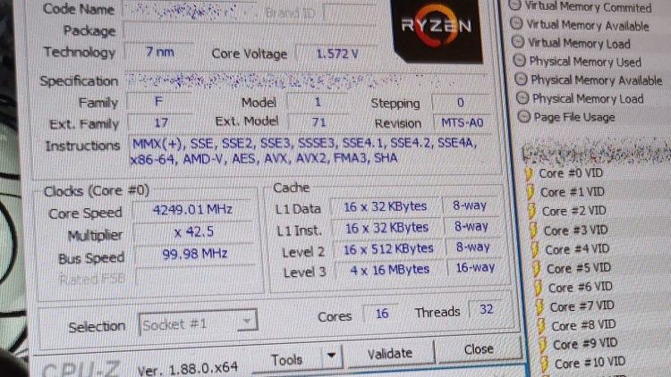
Besides today presentations Ryzen 9 16 cores 32 threads has "supposedly" been benchmarked.

Ryzen-9-2.jpg


Apparently beating (18 core 36 thread) Core i9 9980XE on cinebench.
High voltage suggest it's a heavily overclocked unit.
 
If your code is designed to scale across a large core count, then core-to-core communications have to be mostly eliminated to begin with and the ringbus latency does not matter much. If ringbus latency ruins your software's performance, then either your problem has significant if not severe scaling limitations or your algorithm is poorly designed. For supercomputer code to scale to 100k cores, each thread can't afford to waste more than 0.001% of its time on inter-process communications or blocking the other cores in any way.

That's true only in the case where your threads don't jump between cores, which some OS's (coughWindowscough) will happily do. Should that happen and you have to copy data from one CPU cache to another, then yes, the Ring Bus becomes a problem.

Likewise, if you have an application where multiple threads need to communicate with eachother (say, a game), then you have the same inherent problems.

The case you describe is the typical case for an embarrassingly parallel problem running on an OS where you can expect threads to not jump between cores.
 
Ryzen 9 cinebench "leaked"

With an overclock, the ryzen 3000 16 core crushes the 18 core 7980xe by about 1000cb in cinebench r15.
Cinebench loves cores, so its surprising to see a 16 core beating an 18 core here. I bet the ryzen 3000s improvements make this 16 core great for productivity.
 
  • Like
Reactions: jdwii
That's true only in the case where your threads don't jump between cores, which some OS's (coughWindowscough) will happily do.
If your thread gets bumped between cores, then it got evicted from that core by the OS scheduler so the OS could run something else on that core, its state got moved from core to RAM, then back from RAM to whatever other core it got scheduled to next. Two full context swaps like this cost a couple of microseconds each, which is ~100X worse than the worst ringbus latency. Ringbus is the least of your worries if the OS bumping your threads between cores is causing performance issues.

The OS shouldn't be swapping threads around while there are enough under-used cores available to keep everything running. If you don't want the OS constantly playing musical chair with your threads, use a few less threads than there are cores available. Alternatively, you can use thread processor affinity to force the OS to associate threads with specific cores and button things up yourself, handy if you want to share data through the nearest L2/L3/L4 or RAM in NUMA environments.
 
Ryzen 9 cinebench "leaked"

With an overclock, the ryzen 3000 16 core crushes the 18 core 7980xe by about 1000cb in cinebench r15.
Cinebench loves cores, so its surprising to see a 16 core beating an 18 core here. I bet the ryzen 3000s improvements make this 16 core great for productivity.

As i stated before Zen 2 is probably going to beat Intel in IPC a first since the Athlon days(around 2003) and funny enough like the Pentium 4 vs Athlon days Intel is still hitting higher frequency's. I truly believe Lisa Su has Amd's CPU division being 100% run by engineers instead of marketing idiots. Aiming for IPC over frequency is extremely smart.

Going to benchmark Zen 2 in several applications that demand single threaded performance including Dolphin emulator and older games to see if Amd has matched Intel in IPC.

Icelake is coming in 2021 lol by then Amd should be on Zen 3 or higher and probably on a newer socket. I guess we might see more pluses to Intel's 14nm tech but who knows.

I remember when i told people here that i would bet money that Zen would be a disaster i'm more then happy to be wrong Zen is everything the FX should have been
 
  • Like
Reactions: NightHawkRMX
Status
Not open for further replies.