jimmysmitty :
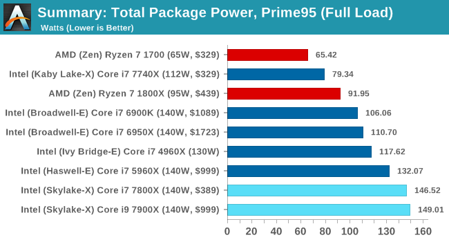
I assume AMDs power numbers might be due to the fact that it is using a low power 14nm, it was designed by Samsung for their mobile chips. It is also why AMD can't clock much higher than their turbo boosts.
However there is nothing saying GFs 7nm will actually be a good process. There is the chance that it flops much like the 20nm flopped for GPUs.
I wouldn't bet on a flop the node market is getting extremely competitive, and AMD has made sure they can hit up different foundries as per their contract!
AMD is rumoured to be fabricating Ryzen CPUs with both Glofo and Samsung
Published: 31st December 2016 | Source: Bits and Chips | Author: Mark Campbell
"
Samsung and Globalfoundries utilise very similar processing technologies for 14nm, with Globalfoundries licensing Samsung's 14nm technology. This means that products that are produced with Globalfoundries, allowing designs to be easily transferred between both foundries if required.
AMD has already confirmed that they are able to produce their silicon products at Samsung if required and has recently updated their supply agreement with Globalfoundries to give them more flexibility when it comes to using other Foundry partners.
This all points to a situation where AMD will be manufacturing their products with both Globalfoundries and Samsung, leaving many to question which foundry is better."
https://www.overclock3d.net/news/cpu_mainboard/amd_is_rumoured_to_be_fabricating_ryzen_cpus_with_both_globalfoundries_and_samsung/1
AMD to Continue Working With TSMC, GLOBALFOUNDRIES on 7 nm Ryzen
by Raevenlord Tuesday, May 16th 2017 19:59
"As it is, AMD has to pay GLOBALFOUNDRIES for its wafer orders that go to other silicon producers (in this case, TSMC), in a quarterly basis since the beginning of 2017, based on the volume of certain wafers purchased from another wafer foundry. In addition, AMD has annual wafer purchase targets from 2016 through the end of 2020, fixed wafer prices for 2016, and a framework for yearly wafer pricing in this amendment, so the company is still bleeding money to GLOBALFOUNDRIES."
https://www.techpowerup.com/233389/amd-to-continue-working-with-tsmc-globalfoundries-on-7-nm-ryzen
Globalfoundries On A Roll With 7nm And 5nm Announcements
JUN 13, 2017 @ 08:00 AM 12,412
"Recently, the fab wars started to heat up between the world’s leading chip manufacturers namely, Globalfoundries, Intel, Samsung and TSMC. Globalfoundries has been making a lot of major announcements including their 22FDX expansion in China in conjunction with the Chengdu government. However, the Chengdu partnership doesn’t really cover leading edge nodes, but more mainstream nodes that are optimized for cost and flexibility at a specific performance and power level.
Hot on the heels of the 5nm announcement in partnership with IBM Research and Samsung, Globalfoundries is making two announcements around its 7nm manufacturing process. While the 5nm process is still in the test phases, Globalfoundries 7nm is much further along. In fact, today, Globalfoundries is announcing that their 7LP (Leading-Performance) process and FX-7 ASIC platform are available today for partners to start planning to utilize with design kits.
Geometry important but not everything
One thing I must mention first- while geometry is still important, it is but only one of many factors in determining a quality fab technology. In the end, what matters is hitting the desired power and performance metrics at the lowest possible cost, regardless if it’s a leading node or not. In addition to geometry, people should also consider die per wafer, die area scaling (i.e. fin pitch, gate pitch, interconnect pitch, cache cell size), transistor performance and leakage, logic area scaling, cost per transistor, and yield, measured by good die per wafer.
7nm, 7LP (Leading Performance) FinFET
Globalfoundries 7nm LP FinFET process could prove to be beneficial for some of Globalfoundries biggest customers like AMD who need the highest performance and density logic and cache memories. Advanced Micro Devices is currently using Globalfoundries 14nm FinFET process to build their new and impressive Ryzen CPUs and APUs. As AMD starts to deliver high performance CPUs and GPUs on a single chip they will need to have as much die area to work with and as low power as they could possibly get. 7nm FinFET would help companies like AMD continue to compete and offer the cutting-edge products that their customers are already starting to expect from them.
The 7LP process is a continuation of Globalfoundries
low power work in previous nodes like 14nm with a focus on cost and power. However, with the introduction of 7LP, Globalfoundries is touting a 40% device performance improvement over 14nm while also talking about reducing power by up to 60%.
Globalfoundries 7LP process uses optical lithography, but is EUV “compatible” if a customer’s designs require it for one reason or another. Globalfoundries also claims an over 30% reduction in die cost with an over 45% reduction in target segments. 7LP is still a 7nm FinFET technology, with an expectation that the company will commercialize it in 2018, which isn’t far off, likely thanks to the strong early customer engagement they’ve seen on it. This process really has potential to steal lower power SoC business from Globalfoundries competitors like TSMC that are also vying for leading-edge node business."
https://www.forbes.com/sites/patrickmoorhead/2017/06/13/globalfoundries-on-a-roll-with-7nm-and-5nm-announcements/#6ce29f234730
Report: Samsung To Focus On Its 6-Nanometer Process Node
June 27, 2017 - Written By Mark Real
"A new report from the South Korean publication The Investor is claiming that Samsung’s foundry division will likely reduce its investments on the 7-nanometer process node and instead focus on its 6-nanometer process technology. The publication added that the mass production of chipsets from the 6-nanometer process node will begin by 2019. This move comes after Samsung’s foundry lost a major customer, Qualcomm, to its biggest rival TSMC."
https://www.androidheadlines.com/2017/06/report-samsung-focus-6-nanometer-process-node.html


