Talking about consumer CPUs? That's largely because they don't run flat-out as much or as hard as people run their GPUs. You're focused on the wrong problem.
And RAM does definitely develop errors at a higher rate than CPUs fail.
I have run most of my PCs "flat out" for the first couple of years of owning them and all of those I still have were still working the last time I had to use them. RAM-wise, the only RAM failures I have personally seen were bad DIMMs out-of-box, some of which low reproduction rate single-bit errors that can take hours to show up on memtest86+. I'd wager that most "developing errors" you speak of could have been caught with a 48h memtest86+ burn-in after purchase.
That's if you want to make it transparent to software. On the other hand, if software is aware that there are two GPUs, it could probably partition the work and data more intelligently.
But if you make the software aware of both GPU's, you'd require more work on the software side to get it to work properly or require ISV's to code for it.
Given the state of SLI/CF and Multi-GPU, I don't see requiring ISV's to program for it as a viable solution.
So you need full transparency where the software won't notice the difference and the drivers will make everything work out somehow.
RDNA3 was an explicit rejection of that idea, or did you not read the article? They said they couldn't make the chiplet approach work by splitting the GCD, which is why they instead decided to move the I/O and L3 cache onto chiplets.
I read the article, they said they couldn't make it work in that iteration, doesn't mean future iterations can't attempt to do it that way.
The fact that CDNA got it to work means that it's only a matter of time with R&D before they get it to work.
GPU Compute is a different problem domain with different data movement patterns. That's why they could use multi-die in that case. And, in point of fact, the MI200 is visible to software as two separate GPUs. They didn't attempt Apple's conceit, but also they don't have an interconnect anywhere near as fast as Apple's.
I'm sure AMD's Radeon Engineers can devise a interconnect as fast as Apple's or faster with lower latency, it's only a matter of time before they decide if it's worth the extra power consumption to have multi-die GCD's communicate via Seamless CrossFire.
When that will happen, who knows, time will tell. But I see it as a future inevitability.
I know that, as you can clearly see from post #20.
"Apple's M1 Ultra shows that even packing like 8 channels of LPDDR5 in-package isn't enough to compete with high-end dGPUs."
We were talking about the generic idea of a high-end iGPU. Regardless of the memory technology, Apple managed to aggregate 800 GB/s of memory bandwidth, which is about 80% of a RTX 4090. And yet, their M1 Ultra iGPU struggles to compete with a RTX 3070.
There's no point in using a serial connection for in-package communication. I do wonder if you might be onto something, except maybe the idea would be to put the memory controller in the base of a LPDDR5 stack. I wonder if that would offer any advantages.
The main difference is that my goals are to move the Memory Controller to be closer to the DIMM connections, w/o using the expensive option of mounting it on the DIMM, this way you shorten the length for the total # of parallel connections, which makes it easier to ramp up DIMM interface speeds.
Yes you lengthen the serial connections, but that was always the design goal.
This way you alleviate the # of connections necessary from your CPU and you open up ALOT more PCIe lanes & high speed I/O lanes to be used with the same pin-count.
But my design goals might be different from what you want.
I read the article, they said they couldn't make it work in that iteration, doesn't mean future iterations can't attempt to do it that way.
The fact that CDNA got it to work means that it's only a matter of time with R&D before they get it to work.
In the supercomputer world, scientists build their algorithms around the target machine's hardware and the data dependencies are tightly controlled for sustained throughput. For conventional 3D rendering, the workloads aren't so neatly packaged and tailor-made to suit wonky architectures, so you run into far more challenging performance scaling issues.
This way you alleviate the # of connections necessary from your CPU and you open up ALOT more PCIe lanes & high speed I/O lanes to be used with the same pin-count.
Not really: a single DDR5-6400 DIMM provides ~50GB/s of memory bandwidth, which is about on par with a 5.0x16 CXL interface and both require 64 data pins: 64 single-ended data pins for DDR5, 16x RX+/RX-/TX+/TX- for PCIe. You save a couple of address pins and that is about it. You do get bidirectional bandwidth though, which may provide some benefits in workloads that have a more balanced read-write profile.
In the supercomputer world, scientists build their algorithms around the target machine's hardware and the data dependencies are tightly controlled for sustained throughput. For conventional 3D rendering, the workloads aren't so neatly packaged and tailor-made to suit wonky architectures, so you run into far more challenging performance scaling issues.
Not really: a single DDR5-6400 DIMM provides ~50GB/s of memory bandwidth, which is about on par with a 5.0x16 CXL interface and both require 64 data pins: 64 single-ended data pins for DDR5, 16x RX+/RX-/TX+/TX- for PCIe. You save a couple of address pins and that is about it. You do get bidirectional bandwidth though, which may provide some benefits in workloads that have a more balanced read-write profile.
The Pin-count reduction from the CPU package frees up ALOT of pins to be used for other things, like more PCIe lanes, or other stuff.
We DON'T want the Memory Controller to sit on the DIMMs, that's TOO expensive and the larger PC industry has more or less agreed against that design, not because of the technical benefits, but because of the cost and the extra e-Waste it induces by having a Memory Controller per DIMM isn't worth the extra cost for Memory.
Let's take a look at Socket SP5 (LGA 6096). That's 6096 pins.
12x DIMMs = 288*12 = 3456 pins
3456 pins / 6096 pins just for all the DIMM slots.
With OMI, you can potentially get 2x DIMM Slots per Independent Memory Controller down to 75 contact pins for the serialized connection.
That's comparing 75 contact pin for a serial connection vs (2*288-pins = 576) contact pins for a longer parallel connection through the CPU's PCB.
Imagine what you can do with the remaining {3006 contact pins = 3456-(75*6)} located on your CPU's PCB.
That's ALOT more PCIe or HSIO you can use for anything you want.
That allows ALOT more flexibility in CPU / System design.
In the era where customers are looking for more connections, moving your CPU's memory controller off onto it's own die and having it sit closer to the DIMMs to lower the latency / distance of the parallel traces would work wonders for increasing the DIMM's connection frequency.
The race to 10,000 MT/s and above is happening, the easiest way to get there is by moving the Memory Controller for the CPU to be closer to the DIMMs.
Given that AMD has shown that they're willing to add Infinity Cache (64 MiB of SRAM) onto the Memory Controllers, that could lower the latency by ALOT and cover for any excess latency added by the SerDes step.
They did this on the GPU side, I can see them going that way on the CPU side in the future.
This would give AMD a competitive advantage on the # of PCIe lanes and other HSIO lanes in the future for anything they want including TR like WorkStation CPUs.
You don't have 576 parallel connections to the CPU: out of the DIMM's 288 pins, almost 200 are grounds simply due to the signal integrity issues that come with single-ended signals crossing a connector. Only about 90 pins carry actual signals that need to be routed to the CPU. On the CPU's end, there are already hundreds of ground pads for handling the 200+A peak core current, so data pins effectively get their ground pins for free.
You don't have 576 parallel connections to the CPU: out of the DIMM's 288 pins, almost 200 are grounds simply due to the signal integrity issues that come with single-ended signals crossing a connector. Only about 90 pins carry actual signals that need to be routed to the CPU. On the CPU's end, there are already hundreds of ground pads for handling the 200+A peak core current, so data pins effectively get their ground pins for free.
You have 576 contact pins going to DRAM supporting the parallel connection, yes, many of them are GND, but they still get connected through the CPU contact pins, to the memory controller.
Go count the # of contact pins for the # of Memory Channels, it's a 1:1 mapping of contacts going to the Memory Controller on the CPU side.
I literally counted the AM4 Contact Pin map and validated that all 576 Contact Pins for 2x DIMM channels are there.
The Data pins aren't free, just as the GND pins aren't free.
And that's a big issue since a giant chunk of the pinout for the CPU PCB Substrate is taken up by Memory Channels, those contacts can be better used for other things.
I have run most of my PCs "flat out" for the first couple of years of owning them and all of those I still have were still working the last time I had to use them.
That was back when Intel didn't face much competition from AMD. Try that now, with a K-series model and a gaming board, and I don't expect you'd fare nearly quite as well.
RAM-wise, the only RAM failures I have personally seen were bad DIMMs out-of-box, some of which low reproduction rate single-bit errors that can take hours to show up on memtest86+.
Nope. I usually let it run overnight, so > 12h on work machines. I've caught errors only on the second pass (which is a couple hours in), but never seen the first error to appear on any subsquent pass. There were a few times I've even let it run over the weekend.
At work, I've seen machines get put into service with zero memory errors and develop them over time. The machines with ECC RAM are easy, because you see the errors start showing up in the logs and then (usually) you just replace the bad DIMMs. In other cases, when a machine without ECC develops stability problems, I've run memtest on it and found bad RAM to be the cause.
But if you make the software aware of both GPU's, you'd require more work on the software side to get it to work properly or require ISV's to code for it.
Given the state of SLI/CF and Multi-GPU, I don't see requiring ISV's to program for it as a viable solution.
If/when GPU performance stagnates, I expect it'll come back. It should be easier than SLI/CF, since it should have better support from Microsoft, the GPU makers, and the 3rd party engines that a lot of games are now using.
Again, CDNA is a completely different animal. It runs different workloads, it's programmed differently, and it has zero graphics engines (except for a media decoder).
Another massive example of a chiplet-based GPU is Intel's Ponte Vecchio, which is also aimed at non-graphics workloads.
Well, the aggregate bandwidth between Navi 31's GCD and its MCDs is about 2x that of Apple's M1 Ultra. So, in some sense they already have. The question is whether it makes sense to put that interconnect in the middle of your GPU. I'm sure the on-die bus of the GCD is running even faster than that, so it could still be a bottleneck.
The other way they could scale is to have multiple GCDs, each with its own memory. That's exactly what MI200 did. I guess the main difference between MI200 and what Apple did is that Apple opted to obscure it from software and make the whole thing appear as a single GPU.
Apple's iGPUs are heavily derived from Imagination's, and it was Apple who claimed it could compete with a RTX 3090 but only delivered a solution with RTX 3070-level performance (yet costing several times as much as a RTX 3090).
The main difference is that my goals are to move the Memory Controller to be closer to the DIMM connections, w/o using the expensive option of mounting it on the DIMM, this way you shorten the length for the total # of parallel connections, which makes it easier to ramp up DIMM interface speeds.
Yes you lengthen the serial connections, but that was always the design goal.
It won't happen. @InvalidError (and what I've been saying for even longer) is right that main DRAM is going to move in-package, with capacity expansion moving out to CXL. Whether there's a minor refactoring that happens around how the CPU interacts with the DRAM stacks is a minor detail, and they're definitely not putting SERDES in the way.
Given that AMD has shown that they're willing to add Infinity Cache (64 MiB of SRAM) onto the Memory Controllers, that could lower the latency by ALOT and cover for any excess latency added by the SerDes step.
No, they didn't. The RDNA3 GPUs' L3 is global and connected with a 883 GB/s parallel link that's about as low-latency as anything off-die can be. It's nothing like what you're proposing.
The only thing we're arguing about here is whether there's a niche big enough for dGPUs. OMI is dead. The sooner you can accept that and move on with your life, the better it's going to be for your mental health.
If/when GPU performance stagnates, I expect it'll come back. It should be easier than SLI/CF, since it should have better support from Microsoft, the GPU makers, and the 3rd party engines that a lot of games are now using.
SLI/CF always affected efficiency, that's the nature of Multi-GPU.
Again, CDNA is a completely different animal. It runs different workloads, it's programmed differently, and it has zero graphics engines (except for a media decoder).
All Ponte Vecchio proves is you can strap more chiplets together.
Well, the aggregate bandwidth between Navi 31's GCD and its MCDs is about 2x that of Apple's M1 Ultra. So, in some sense they already have. The question is whether it makes sense to put that interconnect in the middle of your GPU. I'm sure the on-die bus of the GCD is running even faster than that, so it could still be a bottleneck.
Well, AMD's engineers will figure out how much bandwidth and latency they can tolerate between the interlink.
The other way they could scale is to have multiple GCDs, each with its own memory. That's exactly what MI200 did. I guess the main difference between MI200 and what Apple did is that Apple opted to obscure it from software and make the whole thing appear as a single GPU.
I expect each GCD's to have it's own MCD's but connect the two GCD's via the parallel interface and share all resources.
And I expect AMD to obscure the entire GPU to appear as a single GPU where the end ISV's won't be able to tell the difference.
That's the harder part to get working.
Apple's iGPUs are heavily derived from Imagination's, and it was Apple who claimed it could compete with a RTX 3090 but only delivered a solution with RTX 3070-level performance (yet costing several times as much as a RTX 3090).
It won't happen. @InvalidError (and what I've been saying for even longer) is right that main DRAM is going to move in-package, with capacity expansion moving out to CXL. Whether there's a minor refactoring that happens around how the CPU interacts with the DRAM stacks is a minor detail, and they're definitely not putting SERDES in the way.
And I'm telling you that CXL isn't what you think it is, but we don't need to retread old debates.
You expecting everybody to follow this model of moving the DRAM to on-package isn't feasible for many domains, especially when the customer wants to be able to have their choice of how much RAM they want in their system instead of being forced into a predefined memory config and pay that arbitrary RAM price.
Refactoring how CPU interacts with DRAM is a BIG deal, there are FAR too many software dependencies that are built on top of how CPU interacts with DRAM.
It's a FAR bigger then adding a SerDes layer in between a off CPU Memory Controller that feeds the data back to the CPU.
No, this misunderstands the cache hierarchy of modern CPUs. Putting it off-chip in nearly worthless and makes your solution even more expensive.
And you misunderstand the bigger picture of why I'm doing this and why OMI was conceived in the first place.
No, they didn't. The RDNA3 GPUs' L3 is global and connected with a 883 GB/s parallel link that's about as low-latency as anything off-die can be. It's nothing like what you're proposing.
RDNA3 GPU's L3 might be global in nature, but each Memory Controller's L3 is limited to caching the data from the attached DRAM package, that's a far cry from RDNA2's Infinity cache where it sat on the die and had access to any data on any DRAM package.
That's why I'm not surprised that they're leaving room on their GCD design for a on-die 3D V-Cache SRAM layer.
While the current Infinity Cache is pretty good, it is also kind of limiting in some ways since each 64 MB of Infinity Cache / SRAM can only cache for the DRAM packages attached to it.
That limits how much data you would be caching at any given time since the source of data you have access to is very limited.
That's why I'm not surprised that they're going to probably try to add in another 3D V-cache layer onto the GCD to help alleviate the memory bottle necks.
What I'm proposing is very similar to what they're doing, it's just applied to the CPU side.
Memory Controller off cIOD, closer to DIMM, with SRAM or Infinity cache on Memory Controller.
Maybe even add in another SRAM / 3D V-cache layer on cIOD to help cache some more data.
Basically adding in a L4$ & L5$ to the mix before you even hit RAM.
The only thing we're arguing about here is whether there's a niche big enough for dGPUs. OMI is dead. The sooner you can accept that and move on with your life, the better it's going to be for your mental health.
Nope, not going to accept it, OMI isn't dead; it's part of the CXL consortium. Get used to having OMI at the dinner table, it's part of the family now.
I expect each GCD's to have it's own MCD's but connect the two GCD's via the parallel interface and share all resources.
And I expect AMD to obscure the entire GPU to appear as a single GPU where the end ISV's won't be able to tell the difference.
That's the harder part to get working.
Getting it working isn't the hard part. The problem is making it efficient. If it's not efficient, it's not viable. The way to build a fast GPU is by making it efficient, and that lets you scale up.
Okay, so you're saying multi-die is a failed concept, then? Let's not forget the cheapest machine with it is $5000, and it's just a little desktop mini-PC. Even for Apple, that's not cheap!
You expecting everybody to follow this model of moving the DRAM to on-package isn't feasible for many domains, especially when the customer wants to be able to have their choice of how much RAM they want in their system instead of being forced into a predefined memory config and pay that arbitrary RAM price.
Refactoring how CPU interacts with DRAM is a BIG deal, there are FAR too many software dependencies that are built on top of how CPU interacts with DRAM.
OMI came about because IBM doesn't think about energy efficiency. Coming from their mainframe mindset, they just don't care about stuff like that. Everyone else does, which is why they never showed much interest.
The big difference with CXL is that you don't use CXL.mem by itself. You always have a faster, local memory - be it DDR5 DIMMs or in-package stacks of HBM or LPDDR memory. That's why efficiency doesn't kill you like it would with OMI - because you're not hammering it as hard.
That's just for administrative purposes. They've ceased all development of it and no more products are going to use it. The CXL consortium took on the administrative duties, in exchange for access to the patent portfolio.
You expecting everybody to follow this model of moving the DRAM to on-package isn't feasible for many domains, especially when the customer wants to be able to have their choice of how much RAM they want in their system instead of being forced into a predefined memory config and pay that arbitrary RAM price.
Refactoring how CPU interacts with DRAM is a BIG deal, there are FAR too many software dependencies that are built on top of how CPU interacts with DRAM.
Having 8-64GB of on-package memory doesn't exclude the option of having PCIe/CXL memory expansion cards and some of the ~180 IO pins saved from eliminating the DDRx interface could be re-purposed for PCIe, which would give you 16-40 extra PCIe lanes depending on how generous AMD/Intel are going to be to do whatever you want with instead of having anything dedicated to external memory.
The move to on-package primary DRAM is inevitable, the only question is how long until we get there on mainstream chips. I'd say five years: once performance progression flattens out again, the only way to push single-threaded performance will be to reduce latencies anywhere you can and simplifying designs by eliminating external variables from performance-critical paths. Cores can be optimized around the low latency and high bandwidth of on-package HBM-like memory instead of having to cope with wildly variable external memory which would now be effectively relegated to the role of really fast swapfile.
which would give you 16-40 extra PCIe lanes depending on how generous AMD/Intel are going to be to do whatever you want with instead of having anything dedicated to external memory.
Exactly. This is one of the cool things about CXL, which is that you can use it for memory, storage, networking, accelerators - whatever you want. But, how you partition it is up to you! You could have a compute node with lots of networking and memory, but almost no storage. Or, you could have a storage node with lots of storage and networking, but little memory. It even goes beyond that, by supporting a switched-fabric, which enables flexible bandwidth allocation, as well.
Define "mainstream". Principally: laptop or desktop? Entry-level or gaming tier?
I think some laptop CPUs will first have it by Arrow Lake or Lunar Lake (Intel), and either in AMD's Zen 5 APUs or the gen after that. Desktops will probably lag by a couple generations. AMD might have APUs with in-package DRAM on AM5, but they certainly won't be phasing out DDR5 for CXL.mem until at least AM6. For Intel, I think Lunar Lake is the soonest they would have in-package DRAM on the desktop.
We've seen technologies on laptops that never made it to desktop CPUs, like the eDRAM of Intel's Iris Pro iGPUs, from their Haswell and Broadwell generations. Other examples, like their GNA and IPU, also started in their laptop SoCs and show Intel isn't afraid to innovate there.
As I've said before, you overestimate how much these latency reductions really help most workloads. Not only that, but Apple's in-package LPDDR5-6200 latency is actually worse than Alder Lake's DDR5-4800 latency. So, merely moving the memory in-package is good for power savings and bandwidth (i.e. by making it easier to widen your memory bus), but not really latency.
Cores can be optimized around the low latency and high bandwidth of on-package HBM-like memory instead of having to cope with wildly variable external memory
Even if the latency were lower, you still have lots of cores/threads contending for it. It wouldn't let you get rid of deep out-of-order buffers, or anything like that.
Getting it working isn't the hard part. The problem is making it efficient. If it's not efficient, it's not viable. The way to build a fast GPU is by making it efficient, and that lets you scale up.
If that was the case, monolithic would be the only solution, and chiplets wouldn't be viable, yet here we are, in the age of chiplets.
Everything is going chiplets, and you're going to have to accept some loss in efficiency to gain the benefits of chiplets.
They'll get Multi-GCD working eventually, it's only a matter of time.
Okay, so you're saying multi-die is a failed concept, then? Let's not forget the cheapest machine with it is $5000, and it's just a little desktop mini-PC. Even for Apple, that's not cheap!
That's because they did that at a APU scale where you package CPU/GPU/SoC and did Multi-Die.
You have 2x large dies bonded together.
That & Apple Tax + Bleeding Edge node.
It is, though. And you're the one who keeps banging on about OMI.
You're the one who's treating CXL as the end all / be all solution of the future.
I don't see it that way, it's a nice to have feature for a standardized protocool for remote usage of resources.
I have lots of reservations about it's usefulness.
No, I don't expect external RAM to disappear. I expect it to take the form of CXL.mem.
I don't see that happening, it's a niche idea to force RAM into a external box and there will be limits on who needs that.
The main usage model will still be CPU's attached to DIMM slots for the forsee-able future.
Just because you have Virtual memory, doesn't mean you don't have dependencies on how RAM works.
OMI came about because IBM doesn't think about energy efficiency. Coming from their mainframe mindset, they just don't care about stuff like that. Everyone else does, which is why they never showed much interest.
OMI came about because the pin count on the CPU socket was getting ridiculous, moving the Memory Controller off-board opened up what you can do with the ridiculous amounts of contact pins you have in modern CPU's and better use what we have.
The ever growing Pin Count on modern sockets is getting larger & more ridiculous.
The big difference with CXL is that you don't use CXL.mem by itself. You always have a faster, local memory - be it DDR5 DIMMs or in-package stacks of HBM or LPDDR memory. That's why efficiency doesn't kill you like it would with OMI - because you're not hammering it as hard.
CXL.mem is just another layer on top for remote access to resources and processing, that alone is going to add latency to your work since you're depending on a remote hardware to do the data processing and feeding back the data across the network.
OMI doesn't worsen the efficiency because it shortens the amount of parallel traces and just adds longer serial traces to use.
It's a engineering design tradeoff, net difference should be about the same.
Use basic logic, look at where the Memory Controller is attached.
You're not going to use data from one set of DRAM chips and cache the data onto L3$ that isn't nearby, that's way too far away.
You're moving the data a greater amount just to sit it on L3$, that's more energy used to move data for limited cache space. Space that the local memory controller will need for it's local cache.
Nope. From the article you linked:
"Wassick spotted the connections on the MCD die."
Never say never, how big of a CPU socket do you expect future server CPU's to get?
When they need 24 DIMM, 36 DIMM, 48 DIMM slots/Memory Channels?
We're only getting more Chiplets for server CPU's, more Cores per CPU, demand for more Memory.
They have a easy engineering solution with OMI that solves their problem right away.
They will all go that route eventually.
Instead of making larger CPU PCB with more contact pins, they'll just make more efficient use of what they have.
It's the path of least resistance and ease of engineering + reuse of cheap mass produce-able chiplets.
That's just for administrative purposes. They've ceased all development of it and no more products are going to use it. The CXL consortium took on the administrative duties, in exchange for access to the patent portfolio.
Only because you don't like the idea and don't see value in it.
I don't see alot more value in CXL.mem, that's going to open a whole can of security vulnerabilities and issues that didn't exist before along with adding latency & complexity that didn't exist. The amount of security issues that comes with remote accessing of resources will probably create so many security headaches that it'd be easier for security to disable it and block it then to solve it, limiting it's usefulness.
As far as CXL.mem and RAM in a add-in card, that's going to be relegated to niche use cases when rack space is limited and that eats up a giant chunk of volume for not much in return compared to adding more server hardware with more attached DIMM slots.
Having 8-64GB of on-package memory doesn't exclude the option of having PCIe/CXL memory expansion cards and some of the ~180 IO pins saved from eliminating the DDRx interface could be re-purposed for PCIe, which would give you 16-40 extra PCIe lanes depending on how generous AMD/Intel are going to be to do whatever you want with instead of having anything dedicated to external memory.
The move to on-package primary DRAM is inevitable, the only question is how long until we get there on mainstream chips. I'd say five years: once performance progression flattens out again, the only way to push single-threaded performance will be to reduce latencies anywhere you can and simplifying designs by eliminating external variables from performance-critical paths. Cores can be optimized around the low latency and high bandwidth of on-package HBM-like memory instead of having to cope with wildly variable external memory which would now be effectively relegated to the role of really fast swapfile.
On-Package DRAM as L4$, that's a easy solution with least amount of engineering necessary.
It's been done in the past, I wouldn't be surprised if they do it again.
But to say that it's going to replace the DIMM and main memory as it exists, I don't see that happening.
DIMMs connected to the Memory Controller that connects to the CPU are going to still exist.
And as you stated, adding more latencies isn't going to help, well adding in remote access to main memory / RAM via CXL.mem isn't going to useful when you have to add in protocol layers of PCIe + CXL.mem just to access remote RAM.
Why would anybody give up Main Memory by adding more protocol layers when you can easily just increase the amount of supported DIMM channels on your MoBo via OMI.
That can easily just open up more slots and give you more Memory Capacity, something everybody wants more of.
No matter how fast on-package memory is, it's memory capacity will be much smaller and finite, despite the speed advantage.
That flexible capacity of DIMM is great, and if on-package L4$ goes bad, replacing CPU is going to be very time costly for server maintenance compared to replacing a DIMM stick.
As I've said before, you overestimate how much these latency reductions really help most workloads. Not only that, but Apple's in-package LPDDR5-6200 latency is actually worse than Alder Lake's DDR5-4800 latency. So, merely moving the memory in-package is good for power savings and bandwidth (i.e. by making it easier to widen your memory bus), but not really latency.
Why is DRAM stuck at 9-10ns of net latency? Because gains in DRAM performance are offset by increasingly large address/data muxes and decoders in slow DRAM process logic. Bringing relatively slow memory and its archaic addressing on-package doesn't change that.
With 3D-stacked memory, DRAM can be divided into more sub-channels, smaller banks to make the decoders and muxes smaller and faster, move some of the slow DRAM logic from the slow DRAM process to the logic die underneath, etc.
Even if the latency were lower, you still have lots of cores/threads contending for it. It wouldn't let you get rid of deep out-of-order buffers, or anything like that.
And next-gen 3D-stacked memory not bound by the limitations of traditional DRAM interfaces would be in a much better position to meet the demands of more threads doing whatever it is they do. A conventional (G)DDRx chip only has one command/data bus for the whole thing and requires a somewhat convoluted encoded command/address bus while a 3D-stacked DRAM chip can be divided in however many interfaces the CPU/GPU designer wants and could be given raw access to command/address bits to eliminate the C/A encode/decode stage at both ends. To simplify IO on both sides, you could even have separate read and write busses which would open up the possibility of simultaneous read and write.
Tight integration opens up many possibilities that wouldn't be practical otherwise.
Five years form now, it'll be cheaper to stuff 16GB on-package than put DIMM slots on a motherboard.
While the amount of on-package memory may be smaller, practically any real-world application actively uses only a subset of its total data set at any given time and on-package memory only needs to be large enough to accommodate that. Anything in excess can be on CXL memory as a glorified swapfile where the extra access time doesn't matter much.
I think some laptop CPUs will first have it by Arrow Lake or Lunar Lake (Intel), and either in AMD's Zen 5 APUs or the gen after that. Desktops will probably lag by a couple generations. AMD might have APUs with in-package DRAM on AM5, but they certainly won't be phasing out DDR5 for CXL.mem until at least AM6. For Intel, I think Lunar Lake is the soonest they would have in-package DRAM on the desktop.
We've seen technologies on laptops that never made it to desktop CPUs, like the eDRAM of Intel's Iris Pro iGPUs, from their Haswell and Broadwell generations. Other examples, like their GNA and IPU, also started in their laptop SoCs and show Intel isn't afraid to innovate there.
eDRAM did make it onto two socketable desktop CPUs: the Broadwell-based i7-5775C and i5-5675C on LGA 1150. The 4c/8t i7-5775C fared well compared to newer Intel CPUs, until 10th gen Comet Lake.
Broadwell has only a few short months to shine before Intel's Skylake architecture is expected to surface. Can its two socketed CPUs steal the spotlight?
Laptops with 4 GB soldered-only memory are still being sold in 2023, so maybe a hypothetical future 8-16 GB L4 cache system would be enough for some users. But they can co-exist with main memory for a long time. DIMMs could die. We now know that CAMM will replace SO-DIMM in laptops within a few years. Something could replace DIMMs eventually, even if it's not CXL/PCIe/M.2.
If we ever see "universal memory" capable of putting terabytes of DRAM-like non-volatile storage in a system, that will also shake things up. A real replacement for DRAM and NAND, not the uncomfortable middle tier occupied by Optane/3D XPoint.
Everything is going chiplets, and you're going to have to accept some loss in efficiency to gain the benefits of chiplets.
They'll get Multi-GCD working eventually, it's only a matter of time.
You still need to be very judicious in whether, where, and how to partition. For instance, isn't it interesting that AMD has so far stuck with monolithic dies, for their APUs?
I'm not saying multi-die rendering won't happen. It just might not be invisible to software. I'm sure Intel announced scaling their gaming GPUs to 2 and 4 chiplets, at one point, but I'm having trouble finding it. Anyway, as for how that's meant to work, perhaps they're planning on relying upon their Deep Link technology, which is designed to scale separate GPUs (i.e. like SLI or Crossfire):
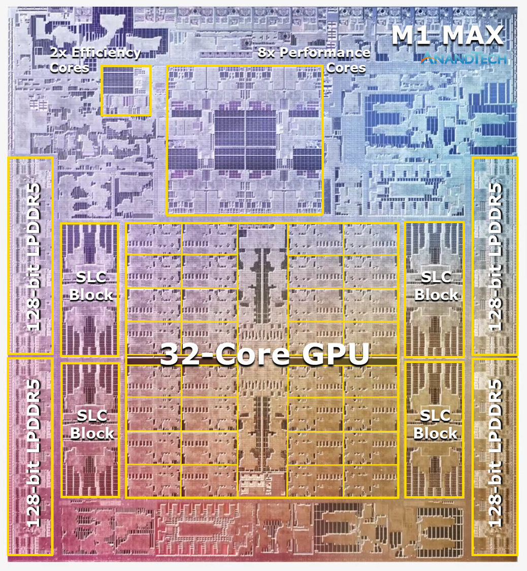
If you look at the floor plan, the M1 Max die is dominated by the GPU + memory controllers + cache + interconnect. Dropping the CPU cores wouldn't change much.
Note they didn't point out where the media codec or NPU sits, but those are typically found on GPU dies. so, we have to consider that some of the unlabelled stuff would still go in a GPU. And, since this graphic was made, we've learned the die-to-die interconnect is that big strip at the bottom. That needs to stay, as well. By my reconing, about 75% of this die would stay, if got rid of the CPU cores and made it a conventional GPU die + interconnect.
Not external. Yeah, people talk about having memory pools as their own box within a rack, but that's indeed niche. The main application is for intra-system connectivity. It seems on track to replace PCIe, in the near future.
OMI came about because the pin count on the CPU socket was getting ridiculous, moving the Memory Controller off-board opened up what you can do with the ridiculous amounts of contact pins you have in modern CPU's and better use what we have.
The ever growing Pin Count on modern sockets is getting larger & more ridiculous.
And what does it tell you that nobody adopted OMI? It should tell you that it either had a fatal flaw, or at least that the sum of its downsides outweighed the benefits.
We keep telling you: they're moving to a combination of in-package + CXL memory. That will let them eliminate the DDR5, while replacing only some of them with more CXL lanes.
You can't argue against an idea you don't understand. So, unless and until you can at least demonstrate an awareness of what we're saying, it's pointless to continue this.
I'll never understand how you seem to think you're smarter than most of the industry, even though you've admitted you're not an EE. They clearly know how to scale up systems. They know how much it costs and how annoying it is to have all those pins and have to route all of the traces. Did you ever ask why they haven't embraced a serial interconnect? Did you ever consider there might be some very rational thinking behind that?
As far as CXL.mem and RAM in a add-in card, that's going to be relegated to niche use cases when rack space is limited and that eats up a giant chunk of volume for not much in return compared to adding more server hardware with more attached DIMM slots.
That's funny, because I'm continually hearing complaints among actual server users and admins that they're running out of RAM for VMs before they run out of CPU cores, in their servers. That tells me memory scaling is a more pressing problem than you think, and probably even higher-priority than scaling up core count.
On-Package DRAM as L4$, that's a easy solution with least amount of engineering necessary.
It's been done in the past, I wouldn't be surprised if they do it again.
But to say that it's going to replace the DIMM and main memory as it exists, I don't see that happening.
That's not a good solution, because in-package HBM has similar latency to external DDR5. Also, hardware-managed cache has both energy & latency overheads.
And as you stated, adding more latencies isn't going to help, well adding in remote access to main memory / RAM via CXL.mem isn't going to useful when you have to add in protocol layers of PCIe + CXL.mem just to access remote RAM.
You obviously don't understand what you're arguing against, here. First, CXL doesn't layer atop PCIe. Second, the protocol is implemented in hardware. There's always some protocol. DDR5 has a protocol. OpenCAPI has a protocol.
If it's not used as L4 cache, but rather directly-addressable DRAM with ECC, then you can have the OS remove pages from use, after they encounter an ECC error. People even do this sort of thing with regular DRAM, today.
Why is DRAM stuck at 9-10ns of net latency? Because gains in DRAM performance are offset by increasingly large address/data muxes and decoders in slow DRAM process logic. Bringing relatively slow memory and its archaic addressing on-package doesn't change that.
With 3D-stacked memory, DRAM can be divided into more sub-channels, smaller banks to make the decoders and muxes smaller and faster, move some of the slow DRAM logic from the slow DRAM process to the logic die underneath, etc.
FWIW, DDR5 halved the channel width and DDR6 is set to do it again. Your explanation is consistent with that, so I'll credit you with maybe having a good point. I hope you're right.
And next-gen 3D-stacked memory not bound by the limitations of traditional DRAM interfaces would be in a much better position to meet the demands of more threads doing whatever it is they do. A conventional (G)DDRx chip only has one command/data bus for the whole thing and requires a somewhat convoluted encoded command/address bus while a 3D-stacked DRAM chip can be divided in however many interfaces the CPU/GPU designer wants and could be given raw access to command/address bits to eliminate the C/A encode/decode stage at both ends. To simplify IO on both sides, you could even have separate read and write busses which would open up the possibility of simultaneous read and write.
Tight integration opens up many possibilities that wouldn't be practical otherwise.
More interesting ideas. I hope these have some mileage, but I'm still skeptical that CPU cores will see such drastic latency reductions that they can be more optimized around them.
Depending how much mileage we get from tighter integration with DRAM, it would be interesting if CPUs could cut back on cache usage. If L2 and L3 could be collapsed into a single system-level cache, then we could get cost savings, energy savings, and latency reductions.
While the amount of on-package memory may be smaller, practically any real-world application actively uses only a subset of its total data set at any given time and on-package memory only needs to be large enough to accommodate that. Anything in excess can be on CXL memory as a glorified swapfile where the extra access time doesn't matter much.
Not only that, but memory compression is viable for a lot of workloads. Things like web browers would benefit hugely from it. Not games or CPU-based rendering, though.
You have 576 contact pins going to DRAM supporting the parallel connection, yes, many of them are GND, but they still get connected through the CPU contact pins, to the memory controller.
Go count the # of contact pins for the # of Memory Channels, it's a 1:1 mapping of contacts going to the Memory Controller on the CPU side.
I literally counted the AM4 Contact Pin map and validated that all 576 Contact Pins for 2x DIMM channels are there.
The Data pins aren't free, just as the GND pins aren't free.
And that's a big issue since a giant chunk of the pinout for the CPU PCB Substrate is taken up by Memory Channels, those contacts can be better used for other things.
FWIW, DDR5 halved the channel width and DDR6 is set to do it again. Your explanation is consistent with that, so I'll credit you with maybe having a good point. I hope you're right.
Stop omitting the GND pins, they are a critical part of the pin count
.
There's a reason why it's called 288-pin DDR5 and not 90-pin or any other pin-count.
Do you want to take a bet on that?
How much are you willing to wager?
While the amount of on-package memory may be smaller, practically any real-world application actively uses only a subset of its total data set at any given time and on-package memory only needs to be large enough to accommodate that. Anything in excess can be on CXL memory as a glorified swapfile where the extra access time doesn't matter much.
Laptops with 4 GB soldered-only memory are still being sold in 2023, so maybe a hypothetical future 8-16 GB L4 cache system would be enough for some users. But they can co-exist with main memory for a long time. DIMMs could die. We now know that CAMM will replace SO-DIMM in laptops within a few years. Something could replace DIMMs eventually, even if it's not CXL/PCIe/M.2.
CAMM seems like a "Form-Factor" replacement for SO-DIMMs due to the Frequency limitations that SO-DIMMs are running into with DDR5.
If we ever see "universal memory" capable of putting terabytes of DRAM-like non-volatile storage in a system, that will also shake things up. A real replacement for DRAM and NAND, not the uncomfortable middle tier occupied by Optane/3D XPoint.
I know they did, I read the same articles as you did.
You still need to be very judicious in whether, where, and how to partition. For instance, isn't it interesting that AMD has so far stuck with monolithic dies, for their APUs?
Yes, because APU's are targeting Thin, Light, Power Efficient LapTops.
It makes sense for that market because of the Power/Latency savings.
I agree with AMD on keeping the mobile market a single monolithic APU.
It works for that market.
I'm not saying multi-die rendering won't happen. It just might not be invisible to software. I'm sure Intel announced scaling their gaming GPUs to 2 and 4 chiplets, at one point, but I'm having trouble finding it. Anyway, as for how that's meant to work, perhaps they're planning on relying upon their Deep Link technology, which is designed to scale separate GPUs (i.e. like SLI or Crossfire):
And I'm saying AMD won't bother introducing it until they can get the software drivers to treat it as "Invisible" to the rest of the software outside.
That's the key point, until that happens, the rest of the hardware work won't matter and they won't bother to implement it.
Invisible Software support is key, that's one of the hard lessons AMD has learned from past mistakes, expecting people to program for your software architecture isn't practical.
Making everything transparent to the software vendors is absolutely key, if you can't get to that point, don't bother implementing it.
The less work the software vendors have to do, the better it is for AMD to get the feature adopted.
If you look at the floor plan, the M1 Max die is dominated by the GPU + memory controllers + cache + interconnect. Dropping the CPU cores wouldn't change much.
It's still a nice chunk of Die-Area + all the supported interconnects that could be saved.
Note they didn't point out where the media codec or NPU sits, but those are typically found on GPU dies. so, we have to consider that some of the unlabelled stuff would still go in a GPU. And, since this graphic was made, we've learned the die-to-die interconnect is that big strip at the bottom. That needs to stay, as well. By my reconing, about 75% of this die would stay, if got rid of the CPU cores and made it a conventional GPU die + interconnect.
And the Navi 31 GCD = 300 mm², still a smaller die than Apple's M1 Max SOC.
And look at how much a RX7900 costs.
I even did a rough estimate of Navi 31 GCD BoM costs on TSMC 5N
It comes out to $100.13/die using 5N, that's not accounting for yields, binning, testing, & packaging/assembly which will drive up costs a bit from that base price.
It's not me - it's the industry. CXL eclipsed literally everything else out there. It killed off Gen-Z and CCIX, too.
And OMI joined the CXL consortium as a technology option for people to use.
Not external. Yeah, people talk about having memory pools as their own box within a rack, but that's indeed niche. The main application is for intra-system connectivity. It seems on track to replace PCIe, in the near future.
CXL isn't replacing PCIe, it's running right on top of it and co-existing with it / operating in parallel.
It needs PCIe since PCIe is the physical hardware implementation for communicating between devices.
You get to choose which protocol to go through, PCIe or CXL, but the PCIe hardware layer and all it's wrappings has to be there for CXL to even work.
So PCIe ain't going to be going anywhere soon, in fact, it's even more critical than ever and everything in the world is going to intercommunicate through PCIe or use the vendor agnostic protocols of CXL.
In this article, we discuss what Compute Express Link or CXL is and why the next-generation of servers will start an industry transformation
www.servethehome.com
Compute Express Link is a cache-coherent link meant to help systems, especially those with accelerators, operate more efficiently. CXL sits atop the PCIe Gen5 link infrastructure. There can be PCIe Gen5 devices, but many PCIe Gen5 (or PCIe 5.0) devices will also support the ability to run lanes in either PCIe or CXL modes. In some ways, this is analogous to how AMD EPYC CPUs can run their I/O lanes as either PCIe or as Infinity Fabric. Instead of being a vendor-specific implementation, this is going to be a broad industry standard. The key advantage of CXL is it allows load/ stores to happen to memory that is directly attached to different endpoints which is what we are going to get into next.
Who knows what Intel's long term plan is, we'll see with them.
And what does it tell you that nobody adopted OMI? It should tell you that it either had a fatal flaw, or at least that the sum of its downsides outweighed the benefits.
Or that people haven't run into the contact-pin limit YET!
Sapphire Rapids is at LGA 4677
Socket SP5 is at LGA 6096.
When we need to change platforms and use new DDR memory standards, we'll see what they choose to do when they need even more memory channels / DIMM channels.
Your emphasis on "remote" seems to be a key point of confusion, here.
The last major functional update to come with AMD new IOD is the Infinity Fabric, AMD’s die-to-die interconnect. On the chiplet-based Ryzen desktop parts, IF is used to provide a low-latency connection between the IOD and the CPU core chiplet(s) on the package.
For the Ryzen 7000 series, AMD has done some further engineering work to reduce the power costs of the IF links, and thus improve the overall power efficiency of the link and reduce the data movement power penalty for using a chiplet-based approach. The most significant thing here is that AMD has doubled the IF link frequency, but cut the physical width of the IF link in half. As a result, Ryzen 7000’s IF links offer the same bandwidth as on Ryzen 5000,
According to AMD, this refactoring is because AMD’s engineers found that, contrary to conventional wisdom, they could save power running a narrower IF link at a higher frequency. Which is to say that, even though higher frequencies are normally power prohibitive, in the case of IF it’s just powering the physical links themselves which is the most expensive part. Part of that shift, in turn, comes from the fact that the newer process nodes have allowed AMD to run the IF link at a lower voltage,
Finally, further reducing AMD’s power consumption here, the IF links on the Ryzen 7000 now support multiple power states, versus the binary on/off states of the IF links on Ryzen 5000 and earlier. This gives AMD a nice middle ground to save power in lighter load situations, by being able to use intermediate states rather than running at full-power just to have an IF link active.
And while this leaves AMD with an obvious (if more power-hungry) route to take for more IF bandwidth in the future should they need it, for now the company intends to stay pat. According to AMD’s engineers, the amount of bandwidth supplied by the Ryzen 7000 IF links, though virtually identical to the amount of bandwidth on the Ryzen 5000 links, is still enough to meet AMD’s die-to-die bandwidth needs – even with extra memory bandwidth afforded by the switch to DDR5.
Less is More, you want less wider links that run faster if you want efficiency.
There is a reason why the rest of the industry went from Parallel Ports to Serial everything.
RAM's interface to DIMM is the last bastion of Parallel connection, IBM's engineers have been harping on that, and it's about efficiency.
How you want to go about it with the SerDes step done on DIMM, or on the MoBo is up to the platform holders.
But most of the industry has stated "NEIN!" to puting the SerDes and Memory Controller on the DIMM.
So that literally leaves the Memory Controller on the MoBo to be a "Buy once, Cry once" solution to get the best of all worlds solutions.
You lower the amount of pins going through your CPU PCB substrate, you still get to keep the entire supply chain of cheapo Parallel Interface DIMMs, you just move the Memory Controller onto the MoBo somewhere, far closer to the DIMM slot.
See above for power savings on connection interface.
Microchip got their Latency Penalty down to ~5 ns, Load Reduced DIMMS got it down to ~(< 4 ns)
In the grand scheme of RAM latency, that's very trivial.
That's how cache works, each 16 MB of SRAM on the MCD caches some of the data for the DRAM attached to it.
Combined it provides better bandwidth
We keep telling you: they're moving to a combination of in-package + CXL memory. That will let them eliminate the DDR5, while replacing only some of them with more CXL lanes.
I know what you're trying to get at, I just don't agree with it.
You can't argue against an idea you don't understand. So, unless and until you can at least demonstrate an awareness of what we're saying, it's pointless to continue this.
I understand it, I just don't agree with it.
If you don't want to debate, we can stop right here.
You seem to be close minded to my ideas of doing things differently.
I'll never understand how you seem to think you're smarter than most of the industry, even though you've admitted you're not an EE. They clearly know how to scale up systems. They know how much it costs and how annoying it is to have all those pins and have to route all of the traces. Did you ever ask why they haven't embraced a serial interconnect? Did you ever consider there might be some very rational thinking behind that?
Did you ever consider that they have multiple stake holders that they are beholden to? That they can't just change the design architecture suddenly.
You don't think the big conglomorates of the RAM industry would like it if their "Bread & Butter money maker DIMMs" were interrupted, do you?
They want to sell more DIMMs of memory, as much as they can, that's how they make their $$$.
The more memory they can sell, the better, if that means more DIMM channels, so be it.
I'm just telling you the writing that's on the wall, because you can't seem to see it.
Funny, I was going to say the same to you about not seeing the seperation of the Memory Controller and the serialization via OMI is a very good thing.
That's funny, because I'm continually hearing complaints among actual server users and admins that they're running out of RAM for VMs before they run out of CPU cores, in their servers. That tells me memory scaling is a more pressing problem than you think, and probably even higher-priority than scaling up core count.
And finding a EASY solution to give you more DIMMs to shove more memory onto the same MoBo is a better solution.
You want 4x the amount of DIMM slots, no problem, we can trade all the existing pin-out for Memory to have 4x the DIMM slots mounted on the server PCB, then you can fill up all the DIMMs with more memory for all your VM's. How does 4x the Memory sound too you?
That's not a good solution, because in-package HBM has similar latency to external DDR5. Also, hardware-managed cache has both energy & latency overheads.
HBM2 has latency between 100-350 ns
DDR4 has 73-107 ns latency for untuned memory.
You obviously don't understand what you're arguing against, here. First, CXL doesn't layer atop PCIe. Second, the protocol is implemented in hardware. There's always some protocol. DDR5 has a protocol. OpenCAPI has a protocol.
In this article, we discuss what Compute Express Link or CXL is and why the next-generation of servers will start an industry transformation
www.servethehome.com
Compute Express Link is a cache-coherent link meant to help systems, especially those with accelerators, operate more efficiently. CXL sits atop the PCIe Gen5 link infrastructure. There can be PCIe Gen5 devices, but many PCIe Gen5 (or PCIe 5.0) devices will also support the ability to run lanes in either PCIe or CXL modes. In some ways, this is analogous to how AMD EPYC CPUs can run their I/O lanes as either PCIe or as Infinity Fabric. Instead of being a vendor-specific implementation, this is going to be a broad industry standard. The key advantage of CXL is it allows load/ stores to happen to memory that is directly attached to different endpoints which is what we are going to get into next.
If it's not used as L4 cache, but rather directly-addressable DRAM with ECC, then you can have the OS remove pages from use, after they encounter an ECC error. People even do this sort of thing with regular DRAM, today.
And then they'll want to replace the faulty hardware, replacing a DIMM stick is easier then swapping out a entire CPU.
Also cheaper depending on the size of the DIMM.


 Twitter