192-layers NAND doesn't have 192 stacked dies. It has the NAND storage array patterns repeated 192 times on a single piece of silicon, no need for TSVs. If DRAM could be designed for manufacturing in a manner similar to NAND, that would allow over 128GB per DRAM chip even if half the DRAM cell density was sacrificed along the way.
Key word in his description: "per package"
You can stack multiple dies of conventional RAM inside one package, be it using TSVs, shingled wire bonding, mezzanine interposers or other means.
I think you still have a problem with cost and power, though.
Not to mention the processing resources and bandwidth needed to actually use it. We're talking RAM - not storage, remember? If you don't have enough bandwidth to even populate all of it between reboots or whatever, then it's pointless to have so much.
An active DRAM chip uses about 250mW while idle chips are around 10mW. If an E3.L card is connected to a 5.0x4 interface and populated with hypothetical 256-layers / 512GB DRAM chips, I doubt more than 1% of it would be active at any given time, so we'd probably be talking just over 1W per chip on average. Fine, that would be only up to about 60 chips per 70W E3.L card instead of 80
Cost-wise, 192-layered NAND is found in TB-scale SSDs under $100, so stacking repeating layers of memory cells clearly isn't particularly expensive for NAND structures. If a similar multi-layered construction was developed for DRAM, I'd say there is a pretty good likelihood it would become much cheaper than any form of die-stacking, especially if it has ECC so the OS can flag pages with flaky bits to avoid them in the future and we accept something like 0.1% capacity loss as normal.
As for actually using this much memory, Frontier has 9.4k nodes at 512GB per CPU + 4x MI250. We are 1/200th of the way there!
I know it's been said before, but I think the sun might finally be setting on the era of "simple programming model; complex hardware". The main reason is energy-efficiency. If hardware exposes more details to the software and vice versa, the end result can be much more efficient.
You might as well tell other programmers to delete their simple programming languages and have everybody come back to c/c++/Rust. https://benchmarksgame-team.pages.debian.net/benchmarksgame/box-plot-summary-charts.html
Those are the most efficient and fastest languages to program for.
There are many junior programmers who don't like Memory Management and will whine/complain.
I'm all for C/C++/Rust, but not everybody is into it.
We didn't need that so much when Moore's Law was in full-effect, but as node improvements taper off, there's going to be renewed enthusiasm for finding performance anywhere you can.
Everybody wants more performance, but some bean counters at top don't care.
Tell that to MS Teams and how their IM client sucks balls and is slow, bloated, and needs to be completely re-written from the ground up.
But upper management doesn't care and won't refactor everything to be properly fast, written in a faster language.
BTW, Vulkan/DX12 is probably the first example of a major increase in programming complexity that went over pretty well with the software community, because they could appreciate the benefits. Don't underestimate just how many low-level details APIs like those already expose about the hardware.
That's also because the target audience, Video Game Devs, cares about performance and asked for those features to be "Console Like" exposure to the hardware.
They got what they requested and games perform better now for the most part, with some caveats.
They'll do it, if/when they think somebody else is about to do it too. There are leaks indicating Intel is going to put a tGPU that's over 3x the size of their biggest laptop iGPU to date in Arrow Lake. It's so big that I think it's going to require at least a chunk of in-package memory to keep it fed. Expect AMD to counter.
We'll see how well it pans out. Right now, AMD's iGPU's are doing good enough for their target audience.
If you want to game, get a dGPU.
And laptops are exactly where it makes the most sense to have things like bigger iGPUs and in-package memory. That's where Apple did it first, and that's where I expect Intel and AMD to do the same. I'm not expecting to see them do anything on par with a high-end laptop dGPU, but just something that extends into the low/mid-range dGPU.
Depends on the target market, if they see normies asking for faster iGPU's, they might listen and AMD will just refresh the iGPU with newer iterations of RDNA to get their performance boosts.
But until then, dGPU's will solve the problem for gaming.
Let's not forget how Intel & AMD already did that Kaby Lake-G Frankenstein that paired a Polaris GPU + HBM on the same "package" as a Kabylake CPU. So, they've already dipped a toe in this water. I think that GPU was about 32 CU, or half of a desktop Vega 64.
I'll believe it when I see it. I don't think AMD feels that threatened in the iGPU market. So far, their solution has been adding a dGPU for gaming, otherwise include a low end dGPU if they really care about that barely faster performance.
You were comparing die costs and omitting nearly half of RX 7900's die area. That's a glaring omission.
It ain't over, till it's over. And I ain't giving up on OMI or the cloned equivalents.
Learn the rules, before you break them. Running against the trend can make sense if you know exactly what you're doing. Otherwise, it tends to go pretty badly.
Ok, now that we're clear on that aspect, can we move on?
Intel is bringing back HBM in their new Xeon Max, but I guess you mean the OmniPath aspect? Intel tried to dominate datacenter networking with OmniPath and the market rejected it. That sent them back to the drawing board and they've since bought Barefoot Networks.
I'm not surprised that HBM is being directly attached on CPU package, it works well for certain data sets and problems.
That also highlights difference, which is that Intel was integrating OmniPath, primarily for inter-node communication. AMD is talking about it for system-level, which means even things like PCIe/CXL.
Intel has been looking at & talking about silicon photonics for a long time. So, definitely expect to hear& see more from them, on that front.
Something unspoken here is what the hell is going to happen to ethernet? Ethernet today is the workhorse of datacenters because of the power and simplicity of fiber optics. I’m still quite a bull for top-of-rack ethernet (hello Inphi/Marvell), but I believe that CXL adoption will encourage PCIe connection within the rack.
I think short-term PCIe adoption will cannibalize 50G ethernet ports, but longer-term, I think that PCIe the fabric is toast. The dream is silicon photonics and CXL combined, and PCIe the fabric is well positioned given its close relation to CXL. I think that PCIe will eventually be superseded by a photonics-based fabric technology, but the protocol will be alive and well. The problem for investors or anyone watching is this is likely on a 10-year time frame.
So in the short term, this could be bad for commodity-like ethernet if it pushes adoption of rack level to interconnect using PCIe, but in the very long time, I think it’s PCIe that’s genuinely at risk. Of course, PCIe could start to adopt more SiPho-like aspects and live, but the jury is still out.
I think PCIe will continue to exist, doesn't matter if it's Copper Based or Silicon Photonics based.
The concept of using the PCIe protocol or any Alt-Mode protocols, like CXL will still be there.
I really think you're confusing it with NVMe, which does have optional support for networking - I think so that it can replace iSCSI.
CXL 3.0 features facilitate the move to distributed, composable architectures and higher performance levels for AI/ML and other compute-intensive or memory-intensive workloads. The CXL 3.0 protocol can support up to 4,096 nodes, go beyond rack. Composable server architectures are when servers are broken apart into their various components and placed in groups where these resources can be dynamically assigned to workloads on the fly. CXL technology continues to enable game-changing innovations for the modern data center at scale.
Meta announced its intentions to incorporate CXL into future server designs, especially for memory-intensive AI applications running in accelerated computing platforms. The company is planning to boost its data center investments by more than 60% this year, with a heavy emphasis on its accelerated computing infrastructure in order to increase engagement on its social media platforms and to lay the foundation for the metaverse. CXL would enable more advanced memory systems that could share memory across various hosts within the network, effectively improving memory utilization, as well as enabling asynchronous sharing of data and results over multiple hosts. The company also proposed the tiering of memory based on applications. For instance, applications such as caching that demand the lowest latency, can use native memory (residing next to the CPU) for "hot" memory pages. This, in contrast with less latency-intensive applications, such as data warehousing, can use CXL memory (riding in PCIe expander cards) for "cold" memory pages as latency, as native memory tends to have 2X better latency than CXL memory. This hierarchy of memory allocation, which can utilize total system memory more effectively, would be beneficial for any accelerated computing platform.
It's a fairly old standard, by now. I think they did it because energy efficiency wasn't an issue at the kinds of speeds they were dealing with, back then, nor was it probably among their primary concerns. These days, you can't afford not to care about it.
I don't think that's the case, the IBM engineers focus was the main issue is scaling of DIMMs and getting more Bandwidth to the CPU by allowing either more DIMM Slots or less DIMM slots an having a flexible OMI port to be used by vendors.
Look at the TDP of IBM mainframe CPUs and tell me energy-efficiency is a priority for them.
IBM POWER10 is IBM's first commercialized processor built using 7nm process technology. IBM Research has been partnering with Samsung Electronics Co., Ltd. on research and development for more than a decade, including demonstration of the semiconductor industry's first 7nm test chips through IBM's Research Alliance.
With this updated technology and a focus on designing for performance and efficiency, IBM POWER10 is expected to deliver up to a 3x gain in processor energy efficiency per socket, increasing workload capacity in the same power envelope as IBM POWER9. This anticipated improvement in capacity is designed to allow IBM POWER10-based systems to support up to 3x increases in users, workloads and OpenShift container density for hybrid cloud workloads as compared to IBM POWER9-based systems. 1
This can affect multiple datacenter attributes to drive greater efficiency and reduce costs, such as space and energy use, while also allowing hybrid cloud users to achieve more work in a smaller footprint.
Experience an integrated media property for tech workers—latest news, explainers and market insights to help stay ahead of the curve.
www.ibm.com
Because of its energy-efficient operation, Power10 can provide many organizations with substantial cost savings and a significantly lower footprint. In a study, IBM compared the footprint of Oracle Database Servers on Power10 with Power 9 and Intel servers. Two Power10 systems can handle the same amount of Oracle workloads as 126 Intel or 3 Power 9 servers. To do this, a Power10 server uses 20 Kw of power compared to 30 Kw for a Power 9 and 102 Kw for the Intel servers. Translated into licenses, a Power10 requires 628 fewer licenses than Intel servers for the studied Oracle workloads.
IBM's Power10 should be competitive with Intel servers, so I wouldn't worry about it.
Everybody measures against Intel.
It's kind of weird how you cast things in a binary terms. System design doesn't work like that. It's an optimization problem, where you're trying to hit competitive performance targets while balancing that against TCO. Because all the performance in the world is of no help if your TCO is uncompetitive. And more pins definitely hurts TCO in both up-front costs and probably also reliability. So, it's definitely not like they don't care about it. They just can't afford to blow their power budget to shave off a couple thousand pins.
Or keep the same # of pins and give you more DIMM slots or more PCIe slots or other forms of HSIO.
It's about making more effective use of what you got.
Because OMI will only become more uncompetitive as DRAM speeds increase.
Best Solution for what problem? What are you trying to solve vs what am I trying to solve?
You're proposing that CXL will magically be a "Cure-All" for everything.
In this tiered memory world, CXL attached pooled memory will be a slower tier of memory compared to DIMMs or even Direct-Attached Memory.
So everybody has it's place.
OMI is a functional subset of CXL. That's why it's a loser. CXL enables switching and pooling, and the article you linked says. This is key for scalability.
OMI is a member of the CXL consortium, but what it solves is vastly different from what CXL is solving.
Both can complement each other just fine. I don't get why you're so narrow minded about my solution.
Like I said before, the future of the datacenter is: in-package memory for bandwidth + CXL.mem for capacity. It has to be this way. You can't get the bandwidth or the energy efficiency with off-package memory, and I already addressed the points about capacity and scalability. Everybody is doing it. Even Nvidia's Grace CPU, in case you missed my earlier post in this thread.
A software person perspective on new upcoming interconnect technologies. Existing Server Landscape Servers are expensive. And difficult to maintain properly. That’s why most people turn to the public cloud for their hosting and computing needs. Dynamic virtual server instances have been key to...
pmem.io
But there’s always a but. In the case of cloud storage, it is latency. Unsurprisingly, that’s also the case for CXL.mem. Memory connected through this interconnect will not be as quick to access as ordinary DIMMs due to inherent protocol costs. Since this is all upcoming technology, no one has yet published an official benchmark that would allow us to quantify the difference. However, it’s expected that the difference will be similar to that of a local vs remote NUMA node access[6]. At least for CXL attached DRAM. That’s still plenty fast. But is it fast enough for applications not to notice if suddenly some of its memory accesses take twice (or more) as long? Only time will tell, but I’m not so sure. For the most part, software that isn’t NUMA-aware doesn’t really scale all that well across sockets.
Be it on-package Memory.
DIMM based Memory.
CXL attached pooled Memory.
Just like we have L0-L3$, we're just adding more layers of Memory/Cache.
Welcome L4-L7, they'll all have it's place based on speed and latency.
You clearly did not read this in its entirety, because it doesn't say a single thing about using it beyond rack-scale. All they talked about was that a server could use it to access memory in another chassis, but no implication was made that memory pools would be shared by large numbers of machines or that they wouldn't be physically adjacent to the machine using them.
Finally, the spec hints at a CXL fabric with the introduction of multi-level switching.
A CXL network fabric will be key to extending the technology beyond the rack level. And there’s reason to believe this could appear in version 3.0 after Gen-Z — not to be confused with the generation of adults born after the turn of the century — donated its coherent-memory fabric assets to the CXL Consortium late last year.
Because CXL.mem is much more flexible. As I've said many times now, it doesn't predetermine your allocation of memory vs. I/O. And, by using switching & pooling, you can scale up capacity almost independent of how many links you opt to use. So, DDR5 DIMM slots will slowly give way to CXL memory slots.
CXL.mem is a tool, it doesn't replace the DIMM, the DIMM will have it's place as the faster tier of memory.
DDR5 DIMM slots will co-exist with DIMM slots as the faster level of memory for instances attached to certain CPU's.
Am I the one being small-minded, here? I keep repeating answers to your questions and it's like you just ignore them and we go around all over again. So, let's review:
Widespread industry support.
Flexible allocation between memory channels and I/O - users get to decide how many lanes they want to use for which purpose, including even legacy PCIe.
One type of controller & PHY, for both memory and PCIe.
Switching enables scaling to larger capacities than a single CPU has lanes.
Pooling enables multiple devices to share a memory pool, without a single CPU becoming a bottleneck.
CXL now supported for chiplet communication, via UCIe.
It's interesting that AMD was also an OpenCAPI member, but never adopted it in any of their products, instead preferring to develop Infinity Link. Maybe that says OpenCAPI itself has deficiencies you don't know about.
Or maybe AMD has different priorities at that moment in time.
You also treat CXL.mem as a magical Silver Bullet, it isn't.
Yes, it's flexible and it can be allocated to any Host on the CXL network.
Doesn't mean there won't be faster memory tiers where certain devices will have priority.
And Faster Memory will always be in demand.
Intel and others have tried and failed in the past to develop a standardized interconnect for accelerators, he tells us. Part of the problem is the complexity associated with these interconnects is shared between the components, making it incredibly difficult to extend them to third parties.
“When we at Intel tried to do this, it was so complex that almost nobody, essentially nobody, was ever able to really get it working,” Pappas reveals. With CXL, essentially all of the complexity is contained within the host CPU, he argues.
This asymmetric complexity isn’t without trade-offs, but Pappas reckons they're more than worth it. These come in the form of application affinity, specifically which accelerator gets priority access to the cache or memory and which has to play second fiddle.
This is mitigated somewhat, Pappas claims, by the fact that customers will generally know which regions of memory the accelerator is going to access versus those accessed by the host. Users will be able to accommodate by setting a bias in the bios[/QUOTE]
I care more about learning than being right. If you have evidence that I'm wrong about something, you're free to share it.
Go read up more on CXL.mem, it isn't the magic bullet you make it out to be.
Is it powerful, sure.
I don't think it's going to replace DIMM slots anytime soon, it's going to co-exist and use DIMM slots as well as use it's own pools of memory allocated from else-where.
Diversity of approaches isn't as important as getting it right. If there are two equally viable approaches, I'm all for having a diversity of options. If one is clearly inferior to the other, then nobody really benefits by keeping the worse approach on some kind of life support.
DIMM makers can't hold back in-package memory.
But DIMM makers will be damned if you try to take away their market.
That's why DIMM slots are critical, and the more, the merrier.
Try telling an architect to mix in some bad design methods or building materials with the good ones they use, and just see how that goes over.
Ecosystems thrive on common standards. That's the Network Effect. When everyone is using PCIe or CXL, then we have interoperability between the widest range of devices and systems. We also get a wide range of suppliers of all the IP and components, which gives device & system designers the widest range of options.
Guess what everybody has, DIMM slots on MoBos.
What does everybody want more of, Memory / RAM?
Everybody wants FASTER access to RAM / Memory!
What's the easy way to get you FASTER RAM/Memory, add in more DIMM slots attached to the CPU.
We've seen this play out with countless standards battles. Once a standard gains dominance and a good bit of momentum, there's a tipping point and the industry shifts to it.
Ok, glad OMI jumped ship to CXL and became part of the team.
You were literally trying to gin up some kind of conspiracy where DIMM vendors would kill the move towards in-package memory. You can't seriously believe that will happen, do you? I don't even see how they could.
They can't stop on-package memory.
They can stop their market of DIMMs from disappearing.
There's a difference.
I just call it like I see it. If you can't handle the idea that your idea might not be the best, or at least that some of us sure don't see it that way, then maybe don't put them out there for people to judge. Forum posts go both ways. You can post whatever you want, but you can't control what other people think of what you post or how they respond. Mainly, I think it's just such a strange thing to have an ego about. It's not even like you're a financial stakeholder in it.
I don't have to be a financial stakeholder in it, I support good ideas, concepts, or companies.
If I like it, I'll support it.
Just like Optane was great tech, I'll still support it even though it's not getting much love right now.
I enjoy reading the the tech news, analyzing the trends, and trying to see where the industry will go. Sometimes I turn out to be wrong, or at least timing-wise, but it's a lot easier to take if you don't get too personally invested in a particular solution.
Oh well, I'm a person who is attached to particular solutions or ideas.
That's just how I am.
For instance, I thought the transition to ARM would happen way faster than it is. I also thought we'd have in-package memory sooner than we will. I thought AMD would be doing better in the AI and GPU-compute space. I didn't predict that Microsoft would come to embrace Linux. I was wrong about all these things, but it doesn't really bother me.
I never thought ARM will take-over the world.
x86 is too entrenched.
ARM will have it's place, but it'll be a small place, right by x86's side.
While RISC-V will be nipping at ARM's market share.
AMD has to battle nVIDIA, that's a up-hill battle.
I didn't see MS embracing Linux either.
So, there's one throw-away remark, made by some author of unknown depth:
"entire data centers might be made to behave like a sinlge system."
That's next to worthless. And yes, they misspelled "single", LOL. There's still nothing to suggest that it will be deployed beyond rack-scale, and that's okay. We don't need a single standard to scale from chiplets to the internet. I know people have done that with Ethernet, but I think those days will soon be behind us.
The whole point of CXL, is to eventually get to DataCenter scale.
That's the point.
Am I the bully? Or maybe you're bullying me, just because I don't agree with you. We keep going around and around, as if you just can't let it go until I agree with you. That's not how the internet works. You simply can't force anyone to agree with you, or else internet arguments would never end.
Ok, if you don't feel like debating anymore, we can end this right now.
You're not convincing me, I'm not convincing you.
I'll be supporting OMI, you go do your thing.
One might appreciate that someone is even taking the time to listen to your ideas and respond to your points. We could just all ignore you. It's not like the world will be any different if you keep clinging to OMI, but I thought you might appreciate understanding why it's being left in the dustbin of history. I didn't realize it was quite so dear to you or that you'd take it so personally.
I don't think it's in the dustbin of history, it just hasn't been utilized yet.
You can't beat CXL, though. That's the problem. OMI loses to DDR5 on energy-efficiency, it loses to in-package memory on bandwidth, and it loses to CXL on scalability and flexibility. That leaves it with no legs left to stand on.
It's not about beating CXL.
That's what I'm trying to tell you.
OMI is a way of connecting more DIMMs, something that is limited by the # of contacts needed on the CPU package and it's excessive growth.
The implementers will make it as efficient as they can to serialize the connection back to the CPU.
And OMI will use DDR5 or the latest DDR# DIMMs.
Or whatever RAM takes over from DDR#.
CXL is about better utilizing the resources you have in the DataCenter.
If ___ memory in RAM isn't being utilized, it can get allocated to another VM.
So if _ memory area in this __ DIMM on this _ CPU host isn't being used, it can get allocated.
Same with any PCIe attached memory. It's just slower memory that is being utilized.
Nothing about OMI & CXL makes it enemies.
I don't get why you seem to see OMI as the enemy to CXL, when they are literally complementary tech that helps each other.
Both can easily co-exist and be used together.
Where are you getting these figures, and are they applicable to DDR5-era DRAM dies?
I find it a little hard to believe that self-refresh of that many cells takes so little power, but I don't really have a good intuition of how much it should take. As for your active power, I wonder why it's so low, yet performance RAM needs heatsinks and even the standard server memory I use @ stock speeds is warm to the touch.
Cost-wise, 192-layered NAND is found in TB-scale SSDs under $100, so stacking repeating layers of memory cells clearly isn't particularly expensive for NAND structures. If a similar multi-layered construction was developed for DRAM,
That's quite a hypothetical, eh? If it were that straight-forward, you'd think someone probably would've done it by now. Not saying it won't happen, but I'm just saying it's a big leap.
The proposition was using 64 bits of address space. So, you're limited to... let's say a single rack. Thanks to CXL (although people would even do similar with PCIe-based clustering), we can easily conceive of a rack that has a mix of compute nodes and memory pools all being shared and mapped into each machine's address space.
The trouble with stuff like that is simply not knowing how well this guy knows what he's talking about. Anyone on the internet can have a podcast/blog and opine on whatever is the buzzword of the day.
I honestly don't see a cache-coherent interconnect making sense beyond rack-scale. If someone at Cray/HPE said otherwise, I'd probably sit up and pay attention. Or maybe if Nvidia said they were scaling up NvLink as a cache-coherent protocol for datacenter-wide networking. Otherwise, I'd have to say a free opinion is worth what you pay for it.
It's interesting how you've taken to diminishing CXL as some kind of second-class PCIe. That doesn't change anything, other than introducing potential confusion when you're talking to people about it. I'd recommend just calling it CXL. Regardless of sharing PCIe's PHY, it's its own thing.
Just because it can doesn't mean it will. If I were designing a protocol, I'd make all the fixed-size fields a lot bigger than I thought they needed to be. Heck, look at hov NVMe allows up to 64k command queues, each with a maximum depth of up to 64k! Does that mean anyone will ever use that many, or make them that deep? No, it probably just means someone decided to use an integral number of bytes for those fields and thought a limit of 256 was too low.
I can see two key issues with trying to use CXL at that scale. The first being the cache-coherency albatross. For shared memory pools to be very useful, you really want that, but it's a performance-killer, if your latency is too high. The second being how tightly-coupled the machines are, and being able to maintain the cluster in a good state across evenst like hardware failures and node reboots. This is where a more loosely-coupled protocol becomes preferable.
Again, they're really just talking about the same old thing as before, with multiple machines sharing memory. I know you underlined the phrase "hosts within the network", but that doesn't stipulate that they'll be tunneling CXL over the network. If that were something people were going to do, then it would be in the official standard.
Please stop trying to google things that seem to support your statements. That's known as "confirmation bias", and it's how conspiracy theories get built. If CXL supported network tunneling or were appropriate to use at datacenter scale, those details wouldn't be hard to find. The CXL consortium would just come right out and make those claims, themselves.
Energy efficiency is poor at such high frequencies, like I've told you about 2 dozen times already. Not only that, but PCIe hit a wall past 32 Gbps, so that doesn't leave OMI much headroom.
Seriously, do you have memory problems, or are you just trolling me by repeating the same points and questions, as if I haven't already answered them? Because I'm pretty sure trolling isn't allowed here, and if you have memory problems then I'll have to treat you accordingly.
It's not enough slower that you need a tier between in-package DRAM and CXL.mem. That would add unnecessary complexity and waste CPU pins, board space, and power.
No, OMI doesn't add much value beyond what CXL can already do. Also, it's not your solution. You clearly had no part in OpenCAPI or the OMI standard. You're just some kind of IBM fanboy, as far as I can gather.
It does, for energy-efficiency. Servers cannot continue scaling without improving efficiency. Go watch Lisa Su's presentation, or at least read WCCFTech's coverage of it and look through all the slides.
Even if 20 kW servers are fine for IBM, it won't be fine when they release their next generation that takes 25 kW, and the generation after that needs 40 kW.
That's what @InvalidError and I have been saying! The difference is that you want to shoehorn more tiers than needed. That's wasteful, which is why it will disappear, quickly.
that’s also the case for CXL.mem. Memory connected through this interconnect will not be as quick to access as ordinary DIMMs due to inherent protocol costs.
Conventional wisdom says that trying to attach system memory to the PCI-Express bus is a bad idea if you care at all about latency. The further the memory
"A CXL network fabric will be key to extending the technology beyond the rack level. And there’s reason to believe this could appear in version 3.0 after Gen-Z ... donated its coherent-memory fabric assets to the CXL Consortium late last year.
The thing to keep in mind about standards is that sometimes they can be like a "stone soup", where there are lots of stakeholders and they each have agendas and are trying to hitch their agenda on the hot standard of the day. So, sometimes things end up in them which are out-of-place and may not actually get widely implemented or used.
With that being said, multi-level switching is pretty key for rack-scale pooling, since it enables both switching inside the chassis and a switch to interconnect them. So, 2-level switching is the minimum you'd want for rack-scale. Beyond that, probably most don't care but were okay to have it in there if it meant getting 2-level.
According to whom? If it really is so, then they would be clear about that. They have no reason to be secretive. And I don't care about whatever "hot takes" some random blogger posts.
They're not enemies, but it's like iGPU vs. dGPU. If you have a big, fast dGPU, then you have no reason to keep using your iGPU. The dGPU does everything the iGPU can, plus a lot more, and faster. CXL is the newer, superior technology, which is why everyone who was on the OpenCAPI ship jumped and went over to CXL. And now that CXL has all the momentum, there wouldn't be a case for anyone to go back to OpenCAPI or OMI.
192-layers NAND doesn't have 192 stacked dies. It has the NAND storage array patterns repeated 192 times on a single piece of silicon, no need for TSVs. If DRAM could be designed for manufacturing in a manner similar to NAND, that would allow over 128GB per DRAM chip even if half the DRAM cell density was sacrificed along the way.
What is 3D NAND? How is it made? As memory and storage experts, Simms have compiled everything you need to know about 3D NAND technology...
www.simms.co.uk
To extend 3D NAND beyond 128 layers, the industry is quietly developing a technology called string stacking. Still, in R&D, string stacking involves the stacking of individual 3D NAND devices on top of each other. For example, if one stacks three 64-layer 3D NAND devices on top of each other, the resulting chip will represent a 192-layer product.
The trick is to link the individual 64-layer devices with some type of interconnecting scheme. This is not a simple technology to develop. Even with string stacking, 3D NAND would top out at or around 300 layers, according to experts.
The trouble with stuff like that is simply not knowing how well this guy knows what he's talking about. Anyone on the internet can have a podcast/blog and opine on whatever is the buzzword of the day.
I honestly don't see a cache-coherent interconnect making sense beyond rack-scale. If someone at Cray/HPE said otherwise, I'd probably sit up and pay attention. Or maybe if Nvidia said they were scaling up NvLink as a cache-coherent protocol for datacenter-wide networking. Otherwise, I'd have to say a free opinion is worth what you pay for it.
It's interesting how you've taken to diminishing CXL as some kind of second-class PCIe. That doesn't change anything, other than introducing potential confusion when you're talking to people about it. I'd recommend just calling it CXL. Regardless of sharing PCIe's PHY, it's its own thing.
It's not a 2nd-class PCIe, it's doing it's own thing. Nothing changes that, but the fact that it relies on PCIe PHY instead of it's own PHY, that means it's renting it's PHY from another standards group. PCI-SIG is just kind enough to give them room to do so, free of charge.
And CXL isn't the only Alt-mode protocol that reuses PCIe PHY.
AMD's xGMI runs over PCIe as a Alt-mode protocol.
Two EPYC 7742 SoCs are interconnected via Socket to Socket Global Memory Interconnect (xGMI) links, part of the Infinity Fabric that connects all the components of the SoC together. In each Rome node configured with the HPE Apollo 9000 system architecture, there are 3 xGMI links using a total of 48 PCIe lanes. With the xGMI link speed set at 16 GT/s, the theoretical throughput for each direction is 96 GB/s (3 links x 16 GT/s x 2 bytes/transfer) without factoring in the encoding for xGMI, since there is no publication from AMD available. However, the expected efficiencies are 66–75%, so the sustained bandwidth per direction will be 63.5–72 GB/s.
Note: The xGMI link speed and width can be adjusted via BIOS setting. The xGMI Link Max Speed can be set to 10.667, 13, 16 or 18 GT/s. Setting it to a lower speed can save uncore power that can be used to increase core frequency or reduce overall power. It will also decrease cross-socket bandwidth and increase cross-socket latency. xGMI Dynamic Link Width Management saves power during periods of low socket-to-socket data traffic by reducing the number of active xGMI lanes per link from 16 to 8.
Note that 18 GT/s is above the PCIe 4.0 transfer rate of 16 GT/s.
Just because it can doesn't mean it will. If I were designing a protocol, I'd make all the fixed-size fields a lot bigger than I thought they needed to be. Heck, look at hov NVMe allows up to 64k command queues, each with a maximum depth of up to 64k! Does that mean anyone will ever use that many, or make them that deep? No, it probably just means someone decided to use an integral number of bytes for those fields and thought a limit of 256 was too low.
Or they can be planing for the future. That's why you set the limits to be so high.
I can see two key issues with trying to use CXL at that scale. The first being the cache-coherency albatross. For shared memory pools to be very useful, you really want that, but it's a performance-killer, if your latency is too high. The second being how tightly-coupled the machines are, and being able to maintain the cluster in a good state across evenst like hardware failures and node reboots. This is where a more loosely-coupled protocol becomes preferable.
That's why there's going to be tiered memory. If you know the latency for a certain type of memory is too high, you just put it as a lower tier of memory.
Conventional wisdom says that trying to attach system memory to the PCI-Express bus is a bad idea if you care at all about latency. The further the memory
www.nextplatform.com
Most CXL memory controllers add about 200 nanoseconds of latency, give or take a few tens of nanoseconds for additional retimers depending on how far away the device is from the CPU, Tavallaei explains. This is right in line with what other early CXL adopters are seeing as well. GigaIO chief executive officer Alan Benjamin tells The Next Platform that most of the CXL memory expansion modules it has seen are closer to 250 nanoseconds of latency than 170 nanoseconds.
Again, they're really just talking about the same old thing as before, with multiple machines sharing memory. I know you underlined the phrase "hosts within the network", but that doesn't stipulate that they'll be tunneling CXL over the network. If that were something people were going to do, then it would be in the official standard.
Importantly CXL will have coherency and a way for a CPU or Accelerator to communicate over fabric to talk to memory outside of its server rack. By enabling this, you can create pools of computing, acceleration, and memory, and it will all work in a large parallel array. That’s the dream, at least.
We are a bit away from that dream, but we are starting to begin the process of a few key technologies and enablers of the most likely future data center topology.
Please stop trying to google things that seem to support your statements. That's known as "confirmation bias", and it's how conspiracy theories get built. If CXL supported network tunneling or were appropriate to use at datacenter scale, those details wouldn't be hard to find. The CXL consortium would just come right out and make those claims, themselves.
Everybody is already talking about DataCenter wide with CXL, that's what everything is building towards.
Energy efficiency is poor at such high frequencies, like I've told you about 2 dozen times already. Not only that, but PCIe hit a wall past 32 Gbps, so that doesn't leave OMI much headroom.
And yet nVIDIA, AMD already have Serial Based solutions for high frequency serial connections.
It's not like they don't use them already to link devices over greater distances.
And PCIe has already announced 7.0 that they will hit 128 GT/s https://pcisig.com/blog/announcing-pcie®-70-specification-doubling-data-rate-128-gts-next-generation-computing
PCIe is well on their way to bigger and faster serial connections.
with PCIe 8.0, 9.0, 10.0 on the future roadmaps.
Seriously, do you have memory problems, or are you just trolling me by repeating the same points and questions, as if I haven't already answered them? Because I'm pretty sure trolling isn't allowed here, and if you have memory problems then I'll have to treat you accordingly.
I'm not trolling you, I could care less about trolling. You just don't seem to see value in differing opinions and treat your solutions like it's a holy grail and everybody else who is different like they don't belong. You're effectively gate-keeping.
Assuming you care about the real wold, you need to worry about energy efficiency, which is a point you keep ignoring.
And I'm telling you, the people who already use Serial Connections to link chips at great distances already have it figured out.
nVIDIA, AMD, Intel already have solutions for connecting devices at those distances.
I don't know why you're so paranoid about Energy Efficiency when they're already running solutions for Chip to Chip connections at those distances, at those speeds.
I didn't say that. It's only a viable alternative, if you pair it with in-package memory.
Or you can just have proper tiered memory, on-package memory, or not.
It's not enough slower that you need a tier between in-package DRAM and CXL.mem. That would add unnecessary complexity and waste CPU pins, board space, and power.
Conventional wisdom says that trying to attach system memory to the PCI-Express bus is a bad idea if you care at all about latency. The further the memory
www.nextplatform.com
However, as Tavallaei points out, this is still an improvement over four-socket or eight-socket systems where applications may have to contend with multiple NUMA hops just because they need the memory. (Although, to be fair, IBM and Intel have added more and faster links between CPUs to reduce the hops and the latencies per hop.)
With that said, many chipmakers are quick to point out that the CXL ecosystem is only now getting off its feet. AMD’s Kurtis Bowman, who serves on the CXL board of directors, tells The Next Platform many of the early CXL proof of concepts and products are using FPGAs or first-gen ASICs that haven’t yet been optimized for latency. With time, he expects latencies to improve considerably.
If CXL vendors can, as they claim, achieve latencies on par with multi-socket systems outside of show-floor demos, it should largely eliminate the need for application or operating system-specific customizations necessary to take advantage of them. Well, at least as far as memory expansion is concerned. As we’ve seen with Optane, CXL memory tiering will almost certainly require some kind of operating system or application support.
This couldn’t come at a better time as sockets grow larger and fitting more DIMMs on a board is getting harder and harder. There are just fewer places to put them. There are dual-socket systems with room for 32 DIMMs, but as chipmakers add more channels to satiate the bandwidth demands of ever higher core counts, this isn’t scalable.
Forget about in-package DRAM, it's going to need it's own tier from regular DRAM, much less in-package DRAM.
There's nothing wrong with that, programs will work around it, as long as they know it's a different memory tier.
Things will be fine with more tiers of memory.
It's not a member. OpenCAPI simply turned over their assets.
Now all of it's assets are part of CXL consortium. So the tools are there for everybody to use.
No, OMI doesn't add much value beyond what CXL can already do. Also, it's not your solution. You clearly had no part in OpenCAPI or the OMI standard. You're just some kind of IBM fanboy, as far as I can gather.
I support good tech, regardless of where it comes from.
And adding more DIMM slots to provide for FASTER main memory will always have value to the DataCenter.
Servers cannot continue scaling without improving efficiency. Go watch Lisa Su's presentation, or at least read WCCFTech's coverage of it and look through all the slides.
I agree, but you're thinking that Serial Connections have petered out, when it really hasn't.
Also the best minds in working on Serial Connections are constantly tuning it for efficiency.
And the Big 3 (AMD, Intel, nVIDIA) are all using High Speed Serial Connections for long distance chip-to-chip connections.
So I don't know why you think they don't have it solved already when they already use it.
Even if 20 kW servers are fine for IBM, it won't be fine when they release their next generation that takes 25 kW, and the generation after that needs 40 kW.
That's what @InvalidError and I have been saying! The difference is that you want to shoehorn more tiers than needed. That's wasteful, which is why it will disappear, quickly.
Why is it wasteful? Just because a new layer gets added doesn't mean it's wasteful.
Should L3$ have disappeared?
For the longest time, L3$ wasn't a thing, until it was. Now it's a staple of the Cache Hierarchy.
Yes, that's why you want to pair it with in-package DRAM. That said, it actually needn't be as bad as they state.
Conventional wisdom says that trying to attach system memory to the PCI-Express bus is a bad idea if you care at all about latency. The further the memory
And not every device / host will have in-package DRAM. there will be accelerator, and other hosts that just don't have that feature.
And they will still work just fine with CXL.
And your in-package DRAM is a finite amount, how many ways can you split it amongst your Multi-core monster CPU?
If you have too many cores, some VM instances might not get in-package DRAM.
At that point, you make do with what you have and use regular DRAM.
It's not the end of the world if you don't have in-package DRAM.
The thing to keep in mind about standards is that sometimes they can be like a "stone soup", where there are lots of stakeholders and they each have agendas and are trying to hitch their agenda on the hot standard of the day. So, sometimes things end up in them which are out-of-place and may not actually get widely implemented or used.
What kind of wierd ass analogy is this? "Stone Soup"? Who drinks Soup made of Stones?
Or they may be all working towards the same goal, have you thought of that?
Data-Center wide Fabric that can pool all resources together, not limited to in System, or in Rack, or Adjacent Racks.
But the entire Data-Center becomes part of the composable Fabric and shares EVERYTHING.
How is that not a good long term goal?
I thought you of all people would be jumping for joy if that was the case.
With that being said, multi-level switching is pretty key for rack-scale pooling, since it enables both switching inside the chassis and a switch to interconnect them. So, 2-level switching is the minimum you'd want for rack-scale. Beyond that, probably most don't care but were okay to have it in there if it meant getting 2-level.
The whole point of the Global Fabric is to let Data Center managers customize their virtualized resources into any composition they want using any architecture they want.
The only limit is what is accessible, the hiearchy, design, etc; all software configurable across countless virtual instances.
I know you'll keep telling yourself that. 10 years from now, you'll probably still be pitching OMI and hoping it somehow catches on.
You claim it's dead, doesn't mean it really is. It's just waiting to be picked up as a solution to a problem.
According to whom? If it really is so, then they would be clear about that. They have no reason to be secretive. And I don't care about whatever "hot takes" some random blogger posts.
So you need the CXL consortium to tell you how it's going to be?
Is that your level of proof that you require?
They're not enemies, but it's like iGPU vs. dGPU. If you have a big, fast dGPU, then you have no reason to keep using your iGPU. The dGPU does everything the iGPU can, plus a lot more, and faster. CXL is the newer, superior technology, which is why everyone who was on the OpenCAPI ship jumped and went over to CXL. And now that CXL has all the momentum, there wouldn't be a case for anyone to go back to OpenCAPI or OMI.
So because it's the new shiny thing on the block, nobody will bother to look at all the other technologies that have joined up?
That's very shallow thinking.
Where are you getting these figures, and are they applicable to DDR5-era DRAM dies?
I find it a little hard to believe that self-refresh of that many cells takes so little power, but I don't really have a good intuition of how much it should take. As for your active power, I wonder why it's so low, yet performance RAM needs heatsinks and even the standard server memory I use @ stock speeds is warm to the touch.
250mW per chip is still 4W per 16-chips DIMM. That will get toasty given almost no useful surface area and almost no airflow in-between especially when the space between DIMMs is completely choked off by heatsinks in a quad-DIMM setup. As for self-refresh power, put your PC on standby, unplug all of your USB stuff and you will see around 5W at the wall, which includes PSU losses, the motherboard's 5VSB LED, the RTC/CMOS power, the LAN chip for wake-on-LAN support, whatever else the motherboard has on 5VSB and all of your DIMMs including their VRM. You won't be feeling any meaningful heat coming from DRAM chips themselves in self-refresh state. After a quick lookup, it seems 20mW is a more typical amount for today's DRAM.
Yes, 256 layers DRAM at 20mW idle each might be problematic as that would be 5W per chip, eclipsing active power. I must have misplaced a digit while doing my idle math earlier. Down to about 12 chips per E3.L card now. Going to need a few more racks
That's quite a hypothetical, eh? If it were that straight-forward, you'd think someone probably would've done it by now. Not saying it won't happen, but I'm just saying it's a big leap.
Decades of nothing but perfect silicon being acceptable for system memory in large part due to consumer stuff having no ECC is going to be tough to break and most of today's DRAM needs can still be met with planar memory without excessive difficulty, albeit at a steep memory channel count cost while the rest can be managed at substantial expense over Infiniband or equivalents. On-package and CPU/GPU/etc.-stacked DRAM is going to put a huge premium on volumetric density where even HBM and HBM-like stacks may not cut it - you don't want heat from your CPU/GPU to have to go through an 8-tall TSV DRAM stack before reaching the IHS, one layer is already a lot of added thermal impedance. A dire need for density, like the 4-16X needed here, usually does a fine job motivating researchers and manufacturers.
BTW, pretty sure the same challenges that are impeding multi-layered DRAM also apply to eDRAM: if you design DRAM cells that don't need to be etched into the base silicon and can be stacked on top of each other like NAND can, you should be able to embed them in the CPU, GPU, etc. die stackup too.
The proposition was using 64 bits of address space. So, you're limited to... let's say a single rack. Thanks to CXL (although people would even do similar with PCIe-based clustering), we can easily conceive of a rack that has a mix of compute nodes and memory pools all being shared and mapped into each machine's address space.
If you cram TBs of RAM in an E3.L form factor, you'd likely want to have the fastest interface possible to read and write it too. As you mentioned earlier, large memory is questionable if you cannot access it and it would already take a minute to scrub through 8TB at 250GB/s on 6.0x16! On a DIMM-less CPU with 256 PCIe lanes, you still need lanes for GPGPUs, storage, networking, etc., leaving enough PCIe for maybe 10 slots per server. I was thinking about 200 servers before but with my little idle TDP oopsie, it is more like 1000 now.
64bits of addressable space is going to take a while to outgrow in any remotely practical manner, even with 256-layers DRAM that won't exist for another 15+ years. (I give it 5-7 years before 2-16 layers RAM becomes a thing out of necessity now that planar density is pretty much maxed out, then another 10 years to reach similar total layer count as today's NAND.)
Yes, 256 layers DRAM at 20mW idle each might be problematic as that would be 5W per chip, eclipsing active power. I must have misplaced a digit while doing my idle math earlier. Down to about 12 chips per E3.L card now. Going to need a few more racks
Decades of nothing but perfect silicon being acceptable for system memory in large part due to consumer stuff having no ECC is going to be tough to break and most of today's DRAM needs can still be met with planar memory without excessive difficulty, albeit at a steep memory channel count cost while the rest can be managed at substantial expense over Infiniband or equivalents. On-package and CPU/GPU/etc.-stacked DRAM is going to put a huge premium on volumetric density where even HBM and HBM-like stacks may not cut it - you don't want heat from your CPU/GPU to have to go through an 8-tall TSV DRAM stack before reaching the IHS, one layer is already a lot of added thermal impedance. A dire need for density, like the 4-16X needed here, usually does a fine job motivating researchers and manufacturers.
BTW, pretty sure the same challenges that are impeding multi-layered DRAM also apply to eDRAM: if you design DRAM cells that don't need to be etched into the base silicon and can be stacked on top of each other like NAND can, you should be able to embed them in the CPU, GPU, etc. die stackup too.
Instead of mounting "On-Top" of the silicon die or "To the side" adjacent to the silicon die, what about mounting it on the back of the PCB where the Silicon lives?
This way the distance the electrons have to travel is as short as possible w/o introducing a thermal barrier on top of the processor in question.
Solid State Active Cooling like Frore AirJet could cool the memory on the backside of the PCB. And given the amount of heat generated from DRAM, Frore AirJet seems to have enough cooling capacity for it.
All you need to do is introduce a new standard for taller stand-offs for your MoBo or a gaping hole on the MoBo Tray for the backside of the MoBo area where the CPU resides and have an area that can cool the backside of the CPU section of the MoBo.
Instead of mounting "On-Top" of the silicon die or "To the side" adjacent to the silicon die, what about mounting it on the back of the PCB where the Silicon lives?
This way the distance the electrons have to travel is as short as possible w/o introducing a thermal barrier on top of the processor in question.
I've seen this done in some embedded devices that have only one DRAM chip and probably don't get very hot. It probably simplifies routing, but I think the benefits are otherwise negligible. Probably doesn't significantly impact power and should have no effect on latency.
All you need to do is introduce a new standard for taller stand-offs for your MoBo or a gaping hole on the MoBo Tray for the backside of the MoBo area where the CPU resides and have an area that can cool the backside of the CPU section of the MoBo.
If you're going to do significant backside cooling, then cases would also need to be designed for more airflow back there.
PCIe 5.0+ and CXL are more sensitive to distance, however. So, it would be interesting if motherboards were fully 2-sided and we could have card slots & other components on both sides. Obviously, that would require cases to be much more symmetrical. Eventually, optical system interconnects will make this a non-issue, but it's interesting to contemplate in the meantime.
Stacking DRAM chips requires a silicon wafer slab for each chip in the package. Multi-layered chips have multiple layers of cells built all on a single silicon slab. Stacking DRAM dies is 100+ microns per TSV die, stacking layers was 4 microns back in the 64-layers NAND days, likely less now.
Instead of mounting "On-Top" of the silicon die or "To the side" adjacent to the silicon die, what about mounting it on the back of the PCB where the Silicon lives?
The sort of memory I had in mind for DRAM-on-logic would be something finer grained than normal HBM and HBM isn't meant to travel off-interposer, so I doubt bottom-of-substrate would be a viable option. HBM also has ~1300 signals, which would be a pretty large amount of extra holes to drill through the substrate.
From what I've read, even PCIe 4.0 needs retimers. Simple repeaters aren't sufficient.
I think it'd be neat to have double-sided boards. With a board the size of mini-ITX or micro-ATX, you could fit a whole contingent PCIe slots, and it might allow for more accessible M.2 slot placement. Although, saying that, I'm aware some boards already have backside M.2 slots.
I think it'd be neat to have double-sided boards. With a board the size of mini-ITX or micro-ATX, you could fit a whole contingent PCIe slots, and it might allow for more accessible M.2 slot placement. Although, saying that, I'm aware some boards already have backside M.2 slots.
Makes me glad that B-series motherboards don't have enough PCIe lanes for me to fear that motherboard manufacturers may go on an M.2 slot infinity war that will drive board prices up another $100 for the benefit of 0.1% of people
Makes me glad that B-series motherboards don't have enough PCIe lanes for me to fear that motherboard manufacturers may go on an M.2 slot infinity war that will drive board prices up another $100 for the benefit of 0.1% of people
I really hate the modern trend of M.2 slots everywhere.
Just give me good ole PCIe slots.
I can convert a PCIe slot with an adapter to take M.2 drives.
You can't easily convert M.2 to take PCIe Slots without a fugly dongle that looks hideous and gets in the way of so many other things in the case.
I really wish MoBo makers would go back to all PCIe Slots.
And lets start replacing all the SATA ports on MoBo's with U.2 ports.
The U.2 ports can at least connect to the U.3 connector that is backwards compatible with everything.
U.3 connector is backwards compatible with U.2, SATA, SAS.
This way we can all move forwards with better drive compatibility and not hold our drives back by limiting the average consumer to SATA or NVMe over M.2.
Honestly, given how flimsy/fragile the M.2 connector is with it's inherent design limit of 50 mating cycles; it's best if everybody moves all SSD's to 1.8" drives with a U.3 compatible connector.
The SATA / SAS / NVME connector that mates with the SFF-8639 U.3 connector all share the same Mating Cycle rating of 10,000 Mating Cycles.
That's far more durable than 50 mating cycles with M.2.
And the average person has a higher chance of screwing up a M.2 connector or the port that it connects to.
M.2 needs to be relegated to mobile and everybody on DeskTop / Server / Enterprise move back to a more reliable connector that works with U.3.
From what I've read, even PCIe 4.0 needs retimers. Simple repeaters aren't sufficient.
I think it'd be neat to have double-sided boards. With a board the size of mini-ITX or micro-ATX, you could fit a whole contingent PCIe slots, and it might allow for more accessible M.2 slot placement. Although, saying that, I'm aware some boards already have backside M.2 slots.
I remember hearing about the chip maker who produces the PCIe re-timers jacking up prices to absurd levels, now we don't see them as often on client MoBo's because of how they want absurd pricing for each re-timer chip.
no thanks, there are no U.2 drives where i am , and the only u.2 to sata cable is $40. id rather have more pcie slots and 1 or 2 nvme slot is just fine
Chicken-and-egg problem, I think. If motherboards had the connectors, consumer U.2 drives would exist and the cables would be cheaper. Conversely, if consumer U.2 drives were more common, motherboards would have the connectors.
Given where we are, I'm not really sure how the impasse gets broken. It doesn't help that the enterprise world is moving on to the very desktop-unfriendly E1.L form factor. : (
Lets not do that. The U.x/SATA standard is kind of clunky, a bit flimsy and the connector is at least twice as large as it needs to be. If you are going to take away 4xSATA ports for one U.2/3, I'd much rather have a clean new compact connector similar to USB's type-E and use adapter cables or backplanes (ex.: "PCIe type-E" to 4x SATA passive break-out) for legacy stuff.
As much as I would like the idea of PCIe slots being directly accessible without having to pop the side panel open, you need to have a backplane for stuff to plug into for that to work, which is a significant added cost for something only a tiny slice of the consumer market might care about. Providing each E.x-slot with at least four PCIe lanes gets expensive too, same goes for U.x as a point-to-point link.
i have a mobo here right beside me that has a u.2 connector on it. the drives were just never available here, even asked and the person in the store had no idea what u.2 was
Is it a first-gen AM4 board? I seem to recall those had it, which was a bit of a head-scratcher. It was as if they predicted it would take off, but you had to wonder where they got such an idea.
Ebay is your friend. You can find a lot of used enterprise drives on there with good write throughput and capacities, and probably a decent bit of life left (although that part is definitely a gamble).
Find many great new & used options and get the best deals for WD Ultrastar DC SN630 3.84TB 3840GB PCIe Gen 3.1 x4 U.2 NVMe 2.5" SSD Low Hour at the best online prices at eBay! Free shipping for many products!
Lets not do that. The U.x/SATA standard is kind of clunky, a bit flimsy and the connector is at least twice as large as it needs to be. If you are going to take away 4xSATA ports for one U.2/3, I'd much rather have a clean new compact connector similar to USB's type-E and use adapter cables or backplanes (ex.: "PCIe type-E" to 4x SATA passive break-out) for legacy stuff.
USB Type-E, is that what you want to call it?
Personally I don't see value in a fatter USB, I'd rather push PCI-SIG's reversible external OCuLink plug
External Reversible OCuLink is already thinner than a USB Type-A port and is 4x PCIe 4.0 lanes wide.
It's also slightly wider than USB Type-A so you can't accidentally plug it into a USB Type-A port.
It's also Reversible like USB Type-C, so you can't plug it in the wrong way.
For reference classical USB Type-A plug is (12 mm Width x 4.5 mm Height), this is for the metal part, not counting the plastic over molding on the outside.
U.2 is already used in the Server/Enterprise domain, why wouldn't we want to use it on the Client side?
- It's not twice as large, it's literally a few mm thinner than SATA
It's slightly deeper than SATA at the cost of being thinner
I think you're thinking of SATA Express as the clunky connector
It's liteally more space efficient than traditional SATA.
For the MoBo space of 2x SATA Dual Port Towers, replace them with 2x U.2 Ports.
You'd get 8x SATA ports out of it, for the space of 4x SATA Ports.
It's literally superior in every way and backwards compatible.
As much as I would like the idea of PCIe slots being directly accessible without having to pop the side panel open, you need to have a backplane for stuff to plug into for that to work, which is a significant added cost for something only a tiny slice of the consumer market might care about. Providing each E.x-slot with at least four PCIe lanes gets expensive too, same goes for U.x as a point-to-point link.
A U.3 Backplane for all your drive needs does add cost, but in the end, the experience of adding or removing drives is THAT much easier / faster / better.
Not having to open up a PC to get your drive out or add in a drive, especially a tool-less experience is worth every penny.
Look at Apple, they're all about User Experience and ease of use.
On our PC side, especially every day client/consumers; why not make adding/removing/swapping drives as "Easy as humanly possible" with least amount of work for the end user?
Our job is to sell them on the idea.
Buy a U.3 Backplane once, Buy Once/Cry Once. Then you're golden for the life of the computer on Data Drive installation/removal/swapping.
It's also time to bring SAS (Seral Attached SCSI) back to the main stream Client / Consumer.
With the advent of NVMe PCIe drives, there's really no reason to keep SAS as Enterprise/Server ONLY.
Especially with EDSFF being proprietary as eff for the Server Side.
Is it a first-gen AM4 board? I seem to recall those had it, which was a bit of a head-scratcher. It was as if they predicted it would take off, but you had to wonder where they got such an idea.
nope its not my friend specially with it comes to things like hdds, who knows how long it would last. and that, as ended and for $220. not worth it id rather get a sata pcie card and new drive. or even an external one.''
A U.3 Backplane for all your drive needs does add cost, but in the end, the experience of adding or removing drives is THAT much easier / better.
Not having to open up a PC to get your drive out or add in a drive, especially a tool-less experience is worth every penny.
I used to like the idea of a front-accessible hot-swap backplane. But, then I thought about how often I ever swap drives and realized all I really care about is a mounting bay that's more accessible than the legacy kind that requires you to remove both side-panels and unfasten 2 screws on each side.
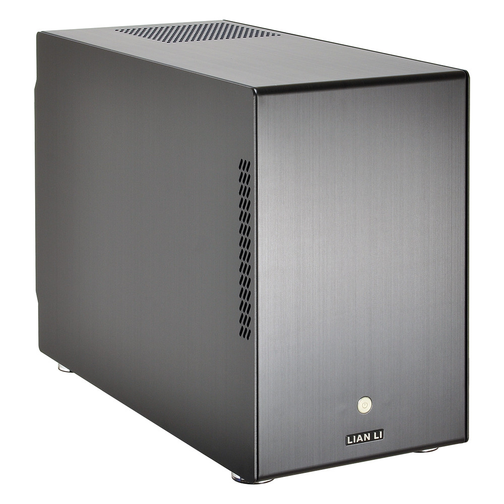
Lian-Li Industrial Co. Ltd announces the PC-M25 chassis. This small form factor (SFF) chassis offers ample storage options and a hot-swap HDD cage for advanced storage applications. The PC-M25 includes a hot-swap HDD rack where users can conveniently install and remove up to five 3.5" drives...
www.techpowerup.com
It offers good airflow, a little bit of vibration-resistance, with the rubber gromets, and it's easy enough to slide drives in and out or change around their cabling.
Vibration-resistance isn't something I've seen in a conventional, front-accessible hotswap setup. Also, my airflow is better, and I'll bet my case is cheaper than it would've been with such a backplane.
i have something similar to This but its made buy Vantec in 2 of my comps, easy-ish access to sata drives with out having to open my case, although the vantec ones i have, require 4 screws to attach the hdd to the tray....
Used enterprise SSDs are a different proposition than used HDDs, because some SSDs are replaced for capacity reasons with still a lot of life remaining. I'm not saying you won't get ripped off, but there's a decent chance you can get a good deal.
I went out of my way to find a Sold listing, so we had a datapoint on the going rate for such drives. If the auction were still open, the current price wouldn't really tell us anything, because the price often shoots up right at the end.
For someone who does a lot of writing, I could see this being compelling. I'm not saying you should buy one like it, but if it's truly got low-hours, then it seems like a pretty good deal to me.


")


 Twitter