AMD's Future Chips & SoC's: News, Info & Rumours.
Page 24 - Seeking answers? Join the Tom's Hardware community: where nearly two million members share solutions and discuss the latest tech.
You are using an out of date browser. It may not display this or other websites correctly.
You should upgrade or use an alternative browser.
You should upgrade or use an alternative browser.
- Status
- Not open for further replies.
juanrga :
You are right. I mixed the 7501 with the 7601. 🙁
Regarding 7601 vs 7551P, 7601 has a small (<10%) advantage in clock speed. That is why a said ALMOST
CheersSince 7601 was tested on single socket, actually almost same performance can be expected from the much cheaper $2100 7551P
Another EPYC review, this time it's the turn of EPYC-7351P
https://www.servethehome.com/amd-epyc-7351p-single-socket-cpu-linux-benchmarks-and-review/
More than the numbers and figures i found interesting last paragraph.
Prediction: considering how good they picture the EPYC-7351P, there will soon be a post by juanrga stating the review is wrong.
https://www.servethehome.com/amd-epyc-7351p-single-socket-cpu-linux-benchmarks-and-review/
More than the numbers and figures i found interesting last paragraph.
We also run our own hosting cluster that is currently all Intel-based. AMD EPYC platform maturity and our experience with the Tyan Transport SX TN70A-B8026 thus far means we will be adding AMD EPYC in the next round of upgrades in Q4 2017/ Q1 2018.
Prediction: considering how good they picture the EPYC-7351P, there will soon be a post by juanrga stating the review is wrong.
aldaia :
Another EPYC review, this time it's the turn of EPYC-7351P
https://www.servethehome.com/amd-epyc-7351p-single-socket-cpu-linux-benchmarks-and-review/
More than the numbers and figures i found interesting last paragraph.
Prediction: considering how good they picture the EPYC-7351P, there will soon be a post by juanrga stating the review is wrong.
https://www.servethehome.com/amd-epyc-7351p-single-socket-cpu-linux-benchmarks-and-review/
More than the numbers and figures i found interesting last paragraph.
We also run our own hosting cluster that is currently all Intel-based. AMD EPYC platform maturity and our experience with the Tyan Transport SX TN70A-B8026 thus far means we will be adding AMD EPYC in the next round of upgrades in Q4 2017/ Q1 2018.
Prediction: considering how good they picture the EPYC-7351P, there will soon be a post by juanrga stating the review is wrong.
From the review:
Here one can take solace in the fact that the AMD EPYC 7351P is not marginally better than the Intel Xeon Silver single (and low-end dual) socket offerings
What AMD essentially did with the EPYC 7351P is put forward a high-performance offering in a price segment where Intel is geared specifically for low power use. To be clear, Intel does have high-performance chips. The sub $1000 CPU segment for Intel is focused solely on low power consumption, not performance.
goldstone77
Distinguished
juanrga :
aldaia :
Another EPYC review, this time it's the turn of EPYC-7351P
https://www.servethehome.com/amd-epyc-7351p-single-socket-cpu-linux-benchmarks-and-review/
More than the numbers and figures i found interesting last paragraph.
Prediction: considering how good they picture the EPYC-7351P, there will soon be a post by juanrga stating the review is wrong.
https://www.servethehome.com/amd-epyc-7351p-single-socket-cpu-linux-benchmarks-and-review/
More than the numbers and figures i found interesting last paragraph.
We also run our own hosting cluster that is currently all Intel-based. AMD EPYC platform maturity and our experience with the Tyan Transport SX TN70A-B8026 thus far means we will be adding AMD EPYC in the next round of upgrades in Q4 2017/ Q1 2018.
Prediction: considering how good they picture the EPYC-7351P, there will soon be a post by juanrga stating the review is wrong.
From the review:
Here one can take solace in the fact that the AMD EPYC 7351P is not marginally better than the Intel Xeon Silver single (and low-end dual) socket offerings
Meaning that everyone can take confort in this distressful sad time of high Intel pricing that EPYC is not slightly better, but significantly better! Those pesky words and their definitions!
sol·ace
noun
1.
comfort or consolation in a time of distress or sadness.
"she sought solace in her religion"
synonyms: comfort, consolation, cheer, support, relief
"they found solace in each other"
mar·gin·al·ly
adverb
to only a limited extent; slightly.
"inflation is predicted to drop marginally"
What AMD essentially did with the EPYC 7351P is put forward a high-performance offering in a price segment where Intel is geared specifically for low power use. To be clear, Intel does have high-performance chips. The sub $1000 CPU segment for Intel is focused solely on low power consumption, not performance.
And that is what we call price to performance advantage!
goldstone77 :
juanrga :
What AMD essentially did with the EPYC 7351P is put forward a high-performance offering in a price segment where Intel is geared specifically for low power use. To be clear, Intel does have high-performance chips. The sub $1000 CPU segment for Intel is focused solely on low power consumption, not performance.
And that is what we call price to performance advantage!
Or a price to power advantage for Intel! The point is that there is not anything revolutionary about this EPYC 7351P. Simply it targets a niche market, that of people that wants performance without spending money on getting performance. Note this 16 core EPYC chip is cheaper (and slower) than a desktop ThreadRipper chip with the same number of cores.
Some quotes from the review, probably most positive review I've ever seen for EPYC:
Make no mistake, the AMD EPYC 7351P performance is very good.
Here you can see a strong showing from the EPYC 7351P which is going to be a recurring theme.
This is a crowded chart, but the raw core count is propelling the AMD EPYC 7351P to some awesome figures. To get above the AMD EPYC 7351P here requires dual Silver 4114 CPUs at nearly 2x the price.
Here the AMD EPYC 7351P falls between the dual socket Intel Xeon Silver 4108 and Silver 4110 configurations. That is a stellar result given both are priced around the same as a single EPYC 7351P.
Again, we see the AMD EPYC 7351P performance shine here putting it near the dual Xeon Silver 4110. That certainly supports AMD’s value proposition on the P series parts. It is also why we are seeing so many vendors enter the market with AMD single-socket servers.
This is certainly an awesome showing for the AMD EPYC 7351P. Intel’s competitive single socket part (price wise) is the Xeon Silver 4114. Figures for that CPU are well below what we are seeing for the EPYC line.
As a result, AMD EPYC supporting AVX2 not AVX-512 is able to keep pace even with Xeon Silver configurations that are 2x or more of the price.
Lots of cores and higher clock speeds help the AMD EPYC here. In fact, the only EPYC that falls below the Intel Xeon Silver 4116 (a $1000 part) in this workload is the AMD EPYC 7251 a $450 part.
As we worked through various other configurations, it became clear that while AMD is very competitive at the high-end, its mainstream offerings are competing with de-featured Xeon Silver CPUs and absolutely obliterate what Intel is offering.
While the EPYC 7351P looks impressive compared to Xeon Silver, we are soon going to show the EPYC 7401(P) numbers that will make you pause.
When discussing about intel 10 nm vs GF 7nm
(i) I can trust Intel data.
In the end you cannot trust Intel data either. Looks like Intel cannon-lake has been delayed to late-2018 reportedly due to 10nm issues.
http://www.digitimes.com/news/a20170920PD207.html
https://www.theinquirer.net/inquirer/news/3017743/intel-reportedly-delays-10nm-cannon-lake-cpus-until-late-2018
https://www.tweaktown.com/news/59209/intel-delays-10nm-cpu-tech-third-time-late-2018/index.html
https://www.neowin.net/news/intels-10nm-cannonlake-processors-delayed-to-late-2018
https://www.dvhardware.net/article67284.html
juanrga :
(i) I can trust Intel data.
In the end you cannot trust Intel data either. Looks like Intel cannon-lake has been delayed to late-2018 reportedly due to 10nm issues.
http://www.digitimes.com/news/a20170920PD207.html
https://www.theinquirer.net/inquirer/news/3017743/intel-reportedly-delays-10nm-cannon-lake-cpus-until-late-2018
https://www.tweaktown.com/news/59209/intel-delays-10nm-cpu-tech-third-time-late-2018/index.html
https://www.neowin.net/news/intels-10nm-cannonlake-processors-delayed-to-late-2018
https://www.dvhardware.net/article67284.html
YoAndy
Reputable
aldaia :
When discussing about intel 10 nm vs GF 7nm
(i) I can trust Intel data.
In the end you cannot trust Intel data either. Looks like Intel cannon-lake has been delayed to late-2018 reportedly due to 10nm issues.
http://www.digitimes.com/news/a20170920PD207.html
https://www.theinquirer.net/inquirer/news/3017743/intel-reportedly-delays-10nm-cannon-lake-cpus-until-late-2018
https://www.tweaktown.com/news/59209/intel-delays-10nm-cpu-tech-third-time-late-2018/index.html
https://www.neowin.net/news/intels-10nm-cannonlake-processors-delayed-to-late-2018
https://www.dvhardware.net/article67284.html
juanrga :
(i) I can trust Intel data.
In the end you cannot trust Intel data either. Looks like Intel cannon-lake has been delayed to late-2018 reportedly due to 10nm issues.
http://www.digitimes.com/news/a20170920PD207.html
https://www.theinquirer.net/inquirer/news/3017743/intel-reportedly-delays-10nm-cannon-lake-cpus-until-late-2018
https://www.tweaktown.com/news/59209/intel-delays-10nm-cpu-tech-third-time-late-2018/index.html
https://www.neowin.net/news/intels-10nm-cannonlake-processors-delayed-to-late-2018
https://www.dvhardware.net/article67284.html
Intel reschedules Cannon Lake launch to year-end 2018, say sources SAY SOURCES ?????? what sources? A guy in a basement?
YoAndy :
aldaia :
When discussing about intel 10 nm vs GF 7nm
(i) I can trust Intel data.
In the end you cannot trust Intel data either. Looks like Intel cannon-lake has been delayed to late-2018 reportedly due to 10nm issues.
http://www.digitimes.com/news/a20170920PD207.html
https://www.theinquirer.net/inquirer/news/3017743/intel-reportedly-delays-10nm-cannon-lake-cpus-until-late-2018
https://www.tweaktown.com/news/59209/intel-delays-10nm-cpu-tech-third-time-late-2018/index.html
https://www.neowin.net/news/intels-10nm-cannonlake-processors-delayed-to-late-2018
https://www.dvhardware.net/article67284.html
juanrga :
(i) I can trust Intel data.
In the end you cannot trust Intel data either. Looks like Intel cannon-lake has been delayed to late-2018 reportedly due to 10nm issues.
http://www.digitimes.com/news/a20170920PD207.html
https://www.theinquirer.net/inquirer/news/3017743/intel-reportedly-delays-10nm-cannon-lake-cpus-until-late-2018
https://www.tweaktown.com/news/59209/intel-delays-10nm-cpu-tech-third-time-late-2018/index.html
https://www.neowin.net/news/intels-10nm-cannonlake-processors-delayed-to-late-2018
https://www.dvhardware.net/article67284.html
Intel reschedules Cannon Lake launch to year-end 2018, say sources SAY SOURCES ?????? what sources? A guy in a basement?
So far is a rumor, you are free to believe it or not, but plenty of sites are reporting it.Intel has reportedly rescheduled the release of its next-generation Cannon Lake-based processors to the end of 2018, which has already affected notebook brand vendors' new projects and their suppliers, according to sources from the upstream supply chain.
Charlie Demerjian already pointed to that possibility a few days ago.
https://semiaccurate.com/2017/09/11/semiaccurate-digs-intels-10nm-process-problems/
People attending GF Tech Symposium today already reported that the rumor mill there suggests it may be true.
Wait and see.
goldstone77
Distinguished
Intel's 10nm Cannonlake processors delayed to late 2018
By John Keefer @@keefinator · 1 hour ago

By John Keefer @@keefinator · 1 hour ago
A slide during the presentation from the Beijing event, spotted by Patently Apple, shows Intel pushing its 10nm process later than previously announced, possibly even into 2019. The 10nm Cannonlakes were originally supposed to start shipping later this year.

DIGITIMESHowever, Intel has reportedly been facing difficulties with its 10nm process. The Cannon Lake processors, originally set for launch in 2017, have seen their launch schedule revised three times: first to the end of 2017 or early 2018, then to the mid-2018, and now the end of 2018, the sources noted.
aldaia :
When discussing about intel 10 nm vs GF 7nm
(i) I can trust Intel data.
In the end you cannot trust Intel data either. Looks like Intel cannon-lake has been delayed to late-2018 reportedly due to 10nm issues.
http://www.digitimes.com/news/a20170920PD207.html
https://www.theinquirer.net/inquirer/news/3017743/intel-reportedly-delays-10nm-cannon-lake-cpus-until-late-2018
https://www.tweaktown.com/news/59209/intel-delays-10nm-cpu-tech-third-time-late-2018/index.html
https://www.neowin.net/news/intels-10nm-cannonlake-processors-delayed-to-late-2018
https://www.dvhardware.net/article67284.html
juanrga :
(i) I can trust Intel data.
In the end you cannot trust Intel data either. Looks like Intel cannon-lake has been delayed to late-2018 reportedly due to 10nm issues.
http://www.digitimes.com/news/a20170920PD207.html
https://www.theinquirer.net/inquirer/news/3017743/intel-reportedly-delays-10nm-cannon-lake-cpus-until-late-2018
https://www.tweaktown.com/news/59209/intel-delays-10nm-cpu-tech-third-time-late-2018/index.html
https://www.neowin.net/news/intels-10nm-cannonlake-processors-delayed-to-late-2018
https://www.dvhardware.net/article67284.html
You are missinterpreting completely what I did mean when I wrote "I can trust Intel data". I mean official parameters for the node, not launch delays due to economic problems, such as insufficient yields. You don't see Intel renaming it 10nm node as 5nm, but you see Glofo renaming its 10nm node as '7nm'.
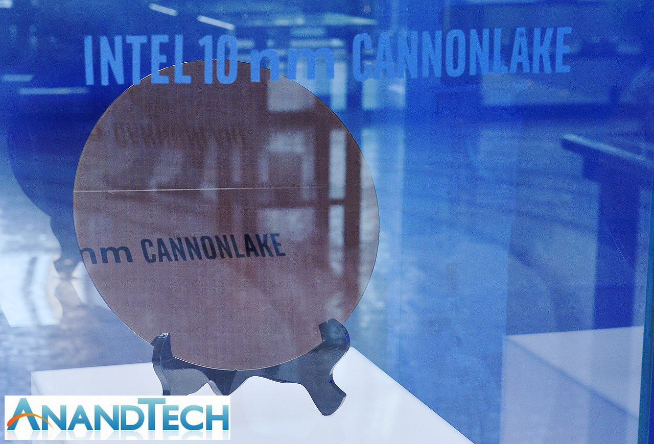
Intel just showed a 10nm wafer of CanonLake chips.
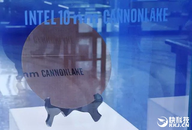
Intel also showed a 10nm wafer of ARM chips.
So far as I know CanonLake chips are in production now. I guess the 'source' guy confounded CannonLake with Icelake. Part of the chips originally named CannonLake were rescheduled as IceLake.
Hellfire13
Titan
goldstone77
Distinguished
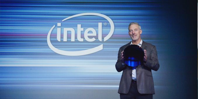
Intel Displays 10nm Wafer, Commits to 10nm ‘Falcon Mesa’ FPGAs
by Ian Cutress on September 19, 2017 8:30 AM EST
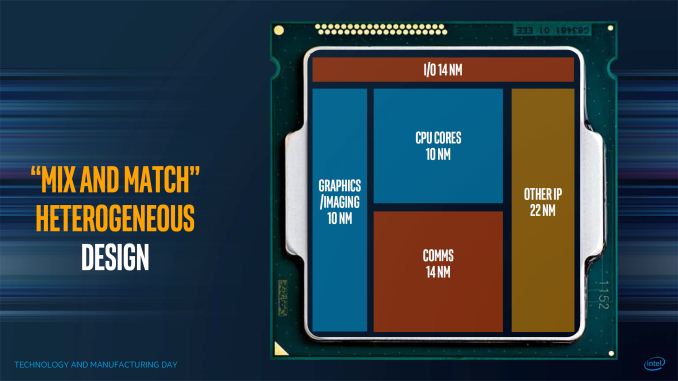


Edit: Could a mod delete this post I moved it to the correct forum.
by Ian Cutress on September 19, 2017 8:30 AM EST

On the back of Intel’s Technology and Manufacturing Day in March, the company presented another iteration of the information at an equivalent event in Beijing this week. Most of the content was fairly similar to the previous TMD, with a few further insights into how some of the technology is progressing. High up on that list would be how Intel is coming along with its own 10nm process, as well as several plans regarding the 10nm product portfolio.
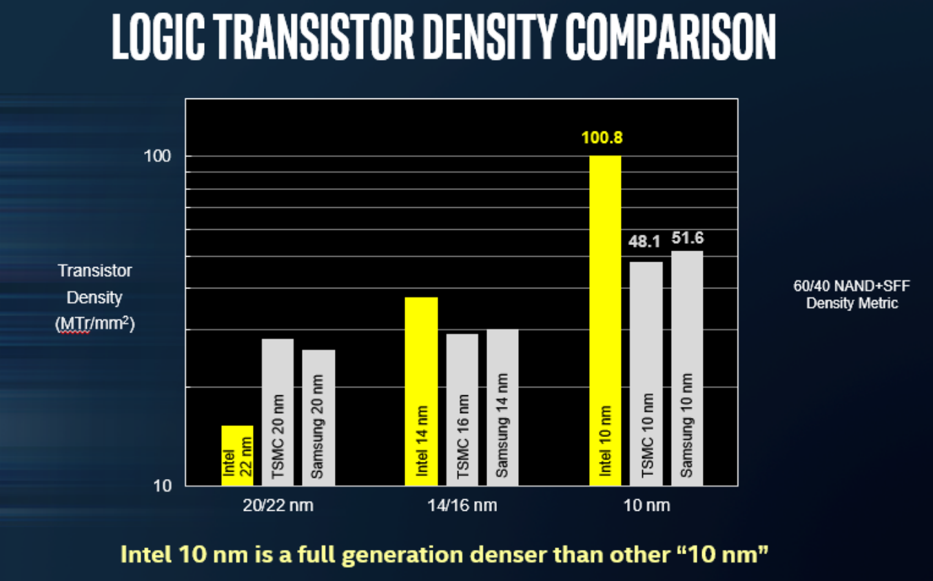
The headline here was ‘we have a wafer’, as shown in the image above. Intel disclosed that this wafer was from a production run of a 10nm test chip containing ARM Cortex A75 cores, implemented with ‘industry standard design flows’, and was built to target a performance level in excess of 3 GHz. Both TSMC and Samsung are shipping their versions of their ‘10nm’ processes, however Intel reiterated the claim that their technology uses tighter transistors and metal pitches for almost double the density of other competing 10nm technologies. While chips such as the Huawei Kirin 970 from TSMC’s 10nm are in the region of 55 million transistors per mm2, Intel is quoting over 100 million per mm2 with their 10nm (and using a new transistor counting methodology).

Intel quoted a 25% better performance and 45% lower power than 14nm, though failed to declare if that was 14nm, 14+, or 14++. Intel also stated that the optimized version of 10nm, 10++, will boost performance 15% or reduce power by 30% from 10nm. Intel’s Custom Foundry business, which will start on 10nm, is offering customers two design platforms on the new technology: 10GP (general purpose) and 10HPM (high performance mobile), with validated IP portfolios to include ARM libraries and POP kits and turnkey services. Intel has yet to announce a major partner in its custom foundry business, and other media outlets are reporting that some major partners that had signed up are now looking elsewhere.
Earlier this year Intel stated that its own first 10nm products would be aiming at the data center first (it has since been clarified that Intel was discussing 10nm++). At the time it was a little confusing, given Intel’s delayed cadence with typical data center products. However, since Intel acquired Altera, it seems appropriate that FPGAs would be the perfect fit here. Large-scale FPGAs, due to their regular repeating units, can take advantage of the smaller manufacturing process and still return reasonable yields by disabling individual gate arrays with defects and appropriate binning. Intel’s next generation of FPGAs will use 10nm, and they will go by the codename “Falcon Mesa”.

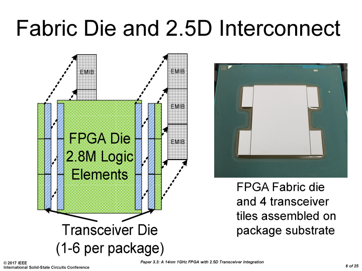
Falcon Mesa will encompass multiple technologies, most noticeably Intel’s second generation of their Embedded Multi-Die Interconnect Bridge (EMIB) packaging. This technology embeds the package with additional silicon substrates, providing a connection between separate active silicon parts much faster than standard packaging methods and much cheaper than using full-blown interposers. The result is a monolithic FPGA in the package, surrounded by memory or IP blocks, perhaps created at a different process node, but all using high-bandwidth EMIB for communication. On a similar theme, Falcon Mesa will also include support for next-generation HBM.

Among the IP blocks that can be embedded via EMIB with the new FPGAs, Intel lists both 112 Gbps serial transceiver links as well as PCIe 4.0 x16 connectivity, with support for data rates up to 16 GT/s per lane for future data center connectivity. This was discussed at the recent Hot Chips conference, in a talk I’d like to get some time to expand in a written piece.
No additional information was released regarding 10nm products for consumer devices.
Additional: 1:00pm September 19th
After doing some digging, we have come across several shots of the wafer up close.

This is from the presentational display. Detail is very hard to make out at the highest resolution we can find this image.
Additional: 1:20pm September 19th
Intel has also now put the presentation up on the website, which gives us this close-up:

Surprisingly, this wafer looks completely bare. Either this is simply a 300mm wafer before production, or Intel have covered the wafer on purpose with a reflective material to stop prying eyes. It's a very odd series of events, as Intel did have other wafers at the event, including 10nm using ARM, and examples of the new 22FFL process.
Additional: 3:00pm September 20th
Intel got back to us with a more detailed Cannon Lake image, clearly showing the separate dies:

Manual counting puts the wafer at around 36 dies across and 35 dies down, which leads to a die size of around 8.2 mm by 8.6 mm, or ~70.5 mm2 per die. At that size, it would suggest we are likely looking at a base dual-core die with graphics: Intel's first 14nm chips in a 2+2 configuration, Broadwell-U, were 82 mm2, so it is likely that we are seeing a 2+2 configuration as well. At that size, we're looking at around 850 dies per wafer.
Edit: Could a mod delete this post I moved it to the correct forum.
Goldstone. Why do you bold the part that says "Surprisingly, this wafer looks completely bare", when in a latter update the same article provides a better photo where the dies can be visible?
Also why do you post Intel information on AMD threads?
Also why do you post Intel information on AMD threads?
goldstone77
Distinguished
GLOBALFOUNDRIES Introduces New 12nm FinFET Technology for High-Performance Applications
-New 12LP technology offers density and performance improvement over current generation -Platform features enhancements for next-gen automotive electronics and RF/analog applications
Santa Clara, Calif., Sept. 20, 2017 (GLOBE NEWSWIRE) -- GLOBALFOUNDRIES today announced plans to introduce a new 12nm Leading-Performance (12LP) FinFET semiconductor manufacturing process. The technology is expected to deliver better density and a performance boost over GF’s current-generation 14nm FinFET offering, satisfying the processing needs of the most demanding compute-intensive applications from artificial intelligence and virtual reality to high-end smartphones and networking infrastructure.
The new 12LP technology provides as much as a 15 percent improvement in circuit density and more than a 10 percent improvement in performance over 16/14nm FinFET solutions on the market today. This positions 12LP to be fully competitive with other 12nm FinFET foundry offerings. The technology leverages GF's expertise at Fab 8 in Saratoga County, N.Y., where its 14nm FinFET platform has been in high-volume production since early 2016.
“The world is in the midst of an unprecedented transition to an era of connected intelligence,” said GF CEO Sanjay Jha. “This new 12LP technology provides the performance and density improvements necessary to help our customers continue innovating at the system level, as they deliver real-time connectivity and edge processing to everything from high-end graphics and automobiles to industrial applications.”
“We are pleased to extend our longstanding relationship with GLOBALFOUNDRIES as a lead customer for their new 12LP technology,” said Mark Papermaster, CTO and senior vice president of technology and engineering, AMD. “Our deep collaboration with GF has helped AMD bring a set of leadership high-performance products to market in 2017 using 14nm FinFET technology. We plan to introduce new client and graphics products based on GF’s 12nm process technology in 2018 as a part of our focus on accelerating our product and technology momentum.”
In addition to transistor-level enhancements, the 12LP platform will include new market-focused features specifically designed for automotive electronics and RF/analog applications—two of the fastest-growing segments in the industry.
Emerging automotive applications in vehicle safety and automated driving require a combination of processing power and extreme reliability. The 12LP platform delivers both, with plans for Automotive Grade 2 qualification at Fab 8 by Q4 2017.
A new RF offering extends the 12LP platform for RF/analog applications such as premium-tier transceivers in sub-6GHz wireless networks. 12LP offers the best scaling in both logic and memory for RF chip architectures with primarily digital and less RF/analog content.
GF's new 12nm FinFET technology complements its existing 12nm FD-SOI offering, 12FDXTM. While some applications require the unsurpassed performance of FinFET transistors, many connected devices need high levels of integration and more flexibility for performance and power consumption, at costs FinFET cannot achieve. 12FDX provides an alternative path for the next generation of connected intelligent systems, enabling the performance of 10nm FinFET with better power consumption, lower cost, and better RF integration than current-generation foundry FinFET offerings.
goldstone77
Distinguished
juanrga :
Goldstone. Why do you bold the part that says "Surprisingly, this wafer looks completely bare", when in a latter update the same article provides a better photo where the dies can be visible?
Also why do you post Intel information on AMD threads?
Also why do you post Intel information on AMD threads?
I posted it in wrong forum on accident!
That's great news... Happy day's. I was kinda waiting for a news release or leak from AMD after the 18 core bench leaks from Intel.
Wasn't expecting anything as good as this though Q1 18...
I guess this will be our Zen+, then Zen 2 on 7nm whenever that happens.
An it's not a low power node. Leading Performance !
That's gonna make a massive difference to clock speeds an performance 😀
Wasn't expecting anything as good as this though Q1 18...
I guess this will be our Zen+, then Zen 2 on 7nm whenever that happens.
An it's not a low power node. Leading Performance !
That's gonna make a massive difference to clock speeds an performance 😀
goldstone77
Distinguished
I guess it's better than 14+... 10% improvement in performance. I can't wait to see what that looks like...
goldstone77
Distinguished
Tesla is working with AMD to develop its own A.I. chip for self-driving cars, says source
Tesla is working with AMD to refine its new chip, which will likely reduce its reliance on Nvidia.
GlobalFoundries CEO Sanjay Jha said it's working with Tesla on a chip.
Tesla has more than 50 employees involved in the project, including chip star Jim Keller.
Tesla working with AMD on A.I. chip for self-driving cars Tesla working with AMD on A.I. chip for self-driving cars
7 Mins Ago | 00:26
Tesla is getting closer to having its own chip for handling autonomous driving tasks in its cars.
The carmaker has received back samples of the first implementation of its processor and is now running tests on it, said a source familiar with the matter.
The effort to build its own chip is in line with Tesla's push to be vertically integrated and decrease reliance on other companies.
But Tesla isn't completely going it alone in chip development, according to the source, and will build on top of AMD intellectual property.
AMD shares spiked after CNBC reported that the company is working with Tesla. Shares of the stock ended the day nearly 5 percent higher and continued to climb after hours.
On Wednesday Sanjay Jha, CEO of AMD spin-off GlobalFoundries, said at the company's technology conference in Santa Clara, California, that the company is working directly with Tesla. GlobalFoundries, which fabricates chips, has a wafer supply agreement in place with AMD through 2020.
A more power-efficient purpose-built chip could help Tesla get closer to delivering totally autonomous driving. Tesla CEO Elon Musk promised this year that capability will be available to consumers in 2019.
Tesla's silicon project is bounding ahead under the leadership of longtime chip architect Jim Keller, the head of Autopilot hardware and software since the departure of Apple veteran Chris Lattner in June. Keller, 57, joined Tesla in early 2016 following two stints at AMD and one at Apple. Keller arrived at Apple in 2008 through its acquisition of Palo Alto Semiconductor and was the designer of Apple's A4 and A5 iPhone chips, among other things.
More than 50 people are working on the initiative under Keller, the source said. Tesla has brought on several AMD veterans after hiring Keller, including director Ganesh Venkataramanan, principal hardware engineer Bill McGee and system circuit design lead Dan Bailey.
AMD and Tesla did not immediately respond to requests for comment.
Current Tesla vehicles use Nvidia graphics processing units as part of the Autopilot self-driving hardware. Previously Tesla used chips from Mobileye, but the two companies parted ways last year after an accident involving a Mobileye-powered Tesla. Earlier this year Intel acquired Mobileye for more than $15 billion.
Notably Tesla is not working with Intel, which has enjoyed a long working relationship with Alphabet's Waymo car group.
As a rule, GPUs from the likes of Nvidia, which are widely used today for various types of AI workloads, are capable of doing many things but aren't designed with just a few narrow computing jobs in mind, hence the custom chip development. Plus, Tesla would be less impacted by pricing dictated by Nvidia if it switches to in-house hardware.
Alphabet has already built two generations of an AI chip that can work as a GPU alternative. Microsoft is working on its own AI chip for the HoloLens. And Apple has incorporated an AI chip into its top-of-the-line iPhone X.
Well that is interesting. They call it vertical integration, but that isn't really at all what they are proposing. Just changing suppliers. Now if Tesla started up their own semiconductor division that would be different.
Tesla powered by Tesla, the marketing practically writes itself! (I know that isn't the chip, had a confusing discussion the other day because of that)
Tesla powered by Tesla, the marketing practically writes itself! (I know that isn't the chip, had a confusing discussion the other day because of that)
- Status
- Not open for further replies.
TRENDING THREADS
-
Review AMD Radeon RX 9070 XT and RX 9070 review: An excellent value, if supply is good
- Started by Admin
- Replies: 163
-
News We need your help to shape the future of Tom’s Hardware
- Started by Admin
- Replies: 83
-
-
News Nvidia RTX 5090's 16-pin power connector hits 150C in reviewer's thermal camera shots
- Started by Admin
- Replies: 20
-
Where to buy AMD's Radeon RX 9070 series graphics cards
- Started by Admin
- Replies: 63
-
Discussion What's your favourite video game you've been playing?
- Started by amdfangirl
- Replies: 4K
-
Review Nvidia GeForce RTX 5070 review: $549 price and performance look decent on paper
- Started by Admin
- Replies: 100

Space.com is part of Future plc, an international media group and leading digital publisher. Visit our corporate site.
© Future Publishing Limited Quay House, The Ambury, Bath BA1 1UA. All rights reserved. England and Wales company registration number 2008885.

