AMD's Future Chips & SoC's: News, Info & Rumours.

Page 25 - Seeking answers? Join the Tom's Hardware community: where nearly two million members share solutions and discuss the latest tech.
Status
Not open for further replies.


Once again. There is no Zen+. This was renamed to Zen2.

There is only Zen, Zen2, and Zen3.

Are you sure about clocks?


It looks as the "14nm+" node was so bad it was canceled. Or was it renamed to 12LP?

Who of you said furing weeks that Zen/VEga 7nm was tapped out this year and would be released next year? Papermaster just disproved that, didn't?

This 12LP is another marketing node

Global-Foundaries-12LP.jpg


This '12nm' node only brings 15% density improvement over 16nm node. A true 12nm shrink would provide 78% improvement. Using the minimal 15% improvement, this 12LP node would have a HD cell density of about 0.061μm², which is very similar to the density of the current 14LPP node.

TSMC "16nm":
48-nm Fin Pitch
90-nm Gate Pitch
64-nm 2D Interconnect Pitch
0.07µm² HD SRAM

GloFo/Samsung "14nm":
48-nm Fin Pitch
78-nm Gate Pitch
64-nm 2D Interconnect Pitch
0.064μm² HD SRAM

Intel "14nm":
42-nm Fin Pitch
70-nm Gate Pitch
52-nm 1D Interconnect Pitch
0.0499μm² HD SRAM

This makes me believe this 12LP is just a rename of the former "14nm+" that appears in AMD slides. The claim this "12LP builds on the GF 14LPP platform" gives even more weight to the hypothesis this 12LP is just a renamed 14nm+.

aHR0cDovL21lZGlhLmJlc3RvZm1pY3JvLmNvbS9HL0cvNjc3MTA0L29yaWdpbmFsLzE1LkpQRw==

10% improvement in performance over TSMC 16nm. Doesn't TSMC 16nm provide more performance than Glofo 14LPP? Ask Nvidia... So 12LP gives, probably, about 5--7% performance improvement over Glofo 14LP? So 100--300MHz extra over current RyZen models? Anyone?

Risk production in H1 2018. Aka volume production in second half of next year, if there are no delays.
 
I got confused. Are they using the "12nm FDSOI" or the "12nm FinFET"? If it's the FinFET, I have to say it smells like 14nm re-labeled for marketing purposes (much like "+" or "++"). I had hopes it was the FDSOI node.

Cheers!


Do you believe that Glofo would announce the same node twice?

The "12nm FDSOI" node is 12FDX. This announcement is about the new 12LP node.

As stated in the slide and in my post, this 12LP is based in 14LPP. Taking a look to the numbers given, it seems evident this 12LP is just a rename of the former "14nm+" node.


Since it's marketing, I am willing to say that a good lie sells better than a bad truth. Hence, the "label" used is "12" and not "14". Same as why Intel used "+" instead of "v2" or "B". There's a plethora of terms that convey "evolution" or "improvement", so, again, I would never ever put it past a good marketing team to put lipstick on a pig and sell it as a pole dancer.

But it seems this "12nm FinFET" has nothing of "FDSOI" in it. Feels like a missed opportunity on one hand and I can't shake off the "stopgap" feeling on the other. Only positive, Zen v1 with a few extra hertz and, I HOPE, fixes or small tweaks.

Cheers!


I think it is pretty evident this "12nm FinFET" has nothing of "FDSOI" in it. Isn't?

So the old plan of first Zen on 2017 then a Richland-like refresh of Zen on 2018 continues, but with some new marketing lies. The bad part is that risk production for 12LP is scheduled to first half of 2018. I expected Pinnacle Ridge to come in first half of 2018, but I am now expecting it in the second half.
 
GLOBALFOUNDRIES Introduces New 12nm FinFET Technology for High-Performance Applications
Sep 20, 2017


New 12LP technology offers density and performance improvement over current generation

Platform features enhancements for next-gen automotive electronics and RF/analog applications

Santa Clara, Calif., Sept. 20, 2017 – GLOBALFOUNDRIES today announced plans to introduce a new 12nm Leading-Performance (12LP) FinFET semiconductor manufacturing process. The technology is expected to deliver better density and a performance boost over GF’s current-generation 14nm FinFET offering, satisfying the processing needs of the most demanding compute-intensive applications from artificial intelligence and virtual reality to high-end smartphones and networking infrastructure.

The new 12LP technology provides as much as a 15 percent improvement in circuit density and more than a 10 percent improvement in performance over 16/14nm FinFET solutions on the market today. This positions 12LP to be fully competitive with other 12nm FinFET foundry offerings. The technology leverages GF's expertise at Fab 8 in Saratoga County, N.Y., where its 14nm FinFET platform has been in high-volume production since early 2016.

“The world is in the midst of an unprecedented transition to an era of connected intelligence,” said GF CEO Sanjay Jha. “This new 12LP technology provides the performance and density improvements necessary to help our customers continue innovating at the system level, as they deliver real-time connectivity and edge processing to everything from high-end graphics and automobiles to industrial applications.”

“We are pleased to extend our longstanding relationship with GLOBALFOUNDRIES as a lead customer for their new 12LP technology,” said Mark Papermaster, CTO and senior vice president of technology and engineering, AMD. “Our deep collaboration with GF has helped AMD bring a set of leadership high-performance products to market in 2017 using 14nm FinFET technology. We plan to introduce new client and graphics products based on GF’s 12nm process technology in 2018 as a part of our focus on accelerating our product and technology momentum.”

In addition to transistor-level enhancements, the 12LP platform will include new market-focused features specifically designed for automotive electronics and RF/analog applications—two of the fastest-growing segments in the industry.

Emerging automotive applications in vehicle safety and automated driving require a combination of processing power and extreme reliability. The 12LP platform delivers both, with plans for Automotive Grade 2 qualification at Fab 8 by Q4 2017.
A new RF offering extends the 12LP platform for RF/analog applications such as premium-tier transceivers in sub-6GHz wireless networks. 12LP offers the best scaling in both logic and memory for RF chip architectures with primarily digital and less RF/analog content.
GF's new 12nm FinFET technology complements its existing 12nm FD-SOI offering, 12FDXTM. While some applications require the unsurpassed performance of FinFET transistors, many connected devices need high levels of integration and more flexibility for performance and power consumption, at costs FinFET cannot achieve. 12FDX provides an alternative path for the next generation of connected intelligent systems, enabling the performance of 10nm FinFET with better power consumption, lower cost, and better RF integration than current-generation foundry FinFET offerings.

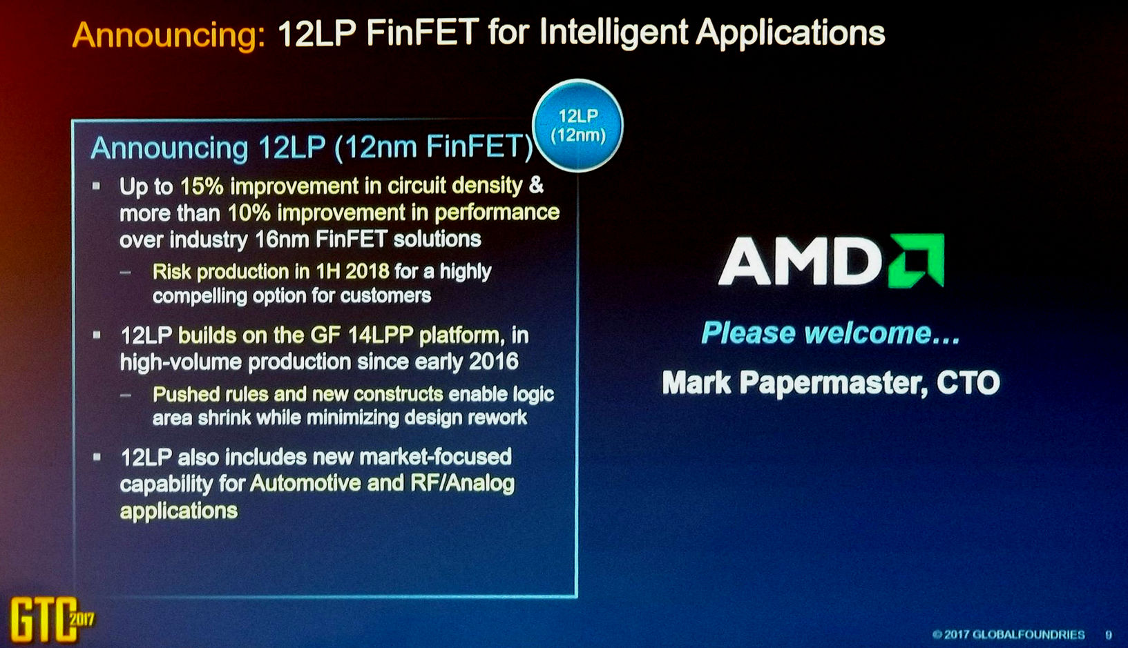
Just the same information from GlobalFoundries
 
More than 10% performance increase that means more than 400mhz... and 15 percent increased density that means more IPC... happy day's.

This is all well an good as long a Intels 10nm is not out.. it's not gonna compete with that. We will need the 7nm glofo node for that job...
Have to wait an see if the rumours are true about 10nm being delayed..
 
12LP technology provides as much as a 15 percent improvement in circuit density and more than a 10 percent improvement in performance over 16/14nm FinFET solutions on the market today.
I'm not encouraged by the wording GlobalFoundries uses with 12nm.
10 percent improvement in performance over 16/14nm FinFET solutions on the market today.
Not really specific here. It doesn't say previous Zen 14nm. I don't know if that is good or bad.
 
I don't care what anyone says no one here expected pinnacle ridge to be on 12nm now i have more confidence that Amd can fight off coffee-lake as long as pinnacle ridge comes out by 2Q 2018.


Always possible all i know is its enough for Amd to compete with coffee-lake i was worried now i'm really not i guess i should wait and see coffee-lake benchmarks but i suspect kabylake/skylake core but with 6 instead of 4 no IPC improvement.

Just to make a dummy comparison at around 4.0ghz Ryzen gives a 162 score in Cinebench R15 where a stock 7700K gets around 194 if Amd can get 15% more performance from IPC+Frequency we are seeing a 186 score

The thing is pinnacle ridge was supposed to just be on 14n+ with no IPC improvements just a small boost in frequency maybe coffee-lake is pushing Amd to accelerate a bit more.
 
Although nothing has been confirmed, 12LP seems to be a rename of 14+. However it is still a nice surprise. A bump in frequency was expected from 14+, the surprise comes from a 15% bump in density, that puts 12LP at the density level of Intel 14nm. If the rumor about Intel 10nm being delayed are true, we will see AMD fighting Intel at a similar technology node during 2018, something not seen in many years.


We all know that, Zen, Zen2 and Zen3 are the architectures
The term "Zen+" has been (unofficially) recycled as a short for "Zen on 14nm+" (maybe to "Zen on 12nm" in the future)
Everybody everywhere uses it instead "Zen on 14nm+" There is no need to post the same again and again every time someone writes "Zen+".


Glofo claims more than 10% performance increase over TSMC 16nm. The performance will be about 5% over Glofo 14nm.

Glofo claims up to 15% density increase over TSMC 16nm. Again we can expect up to 5% density increase over Glofo 14nm.

This 12LP is just a rename of 14LPP+. That is the reason why Glofo is using TSMC as baseline. They cannot use 14LPP as baseline, because this new 12LP is basically the older 14LPP node but with minor tweaks.

Note: Density doesn't not increase IPC. The IPC will be same.


Except that this '12nm' node is not a true 12nm node but a marketing relabel of the 14nm+ node.

We expected Pinnacle Ridge on 14nm+ on the first half of 2018. Now we are expecting Pinnacle Ridge on 14nm+ on the second half of 2018, but with 14nm+ relabeled as '12nm'.

6C CoffeLake comes this year. 8C IceLake comes next year. So 14nm+ 8C Pinnacle Rdige will fight with 10nm 8C IceLake.


TSMC "16nm": 0.07µm² HD SRAM

GloFo/Samsung "14nm": 0.064μm² HD SRAM

Intel "14nm": 0.0499μm² HD SRAM

According to Glofo 12LP gives up to 15% density improvement over TSMC 16nm. So

GloFo "12nm": ~0.061μm² HD SRAM

Which is still 22% behind Intel 14nm.


The problem is that the unofficial nomenclacture can give confusion, because "Zen+" was the originally name for Zen2.

Zen-8.jpg


So if people continue using the term Zen+ to refer to "Zen on 14nm+" it can give to confusions between people has not followed the details and the last renames. That people could believe that Pinnacle Ridge will have higher IPC than Summit Rdige, when the IPC is the same.


I understood it was 15% over GF 14 nm, my bad.

Anyway using memory cells to compare processes is even more misleading that Tr/mm2. Other parts like IO, logic or wiring scale in a very different way. Even Intel discourages using SRAM as a comparison. It is worth pointing out that Intel HD size is purely mentioned for bragging rights, since they are never used. I recently read (unfortunately I don't remember where) that in practice AMD Ryzen L3 cache is 20% denser than Intel Skylake L3 despite that Intel 14 nm is denser than GF 14 nm.


I have to agree guy's I mean I hope it's a shrink but I don't believe it is.. It's 14nm+ renamed..

For the Samsung "Leading Performance" node they use smaller/higher quality transistors this could account for some or most of the 15% extra in the same space (plus refinement in the node/process). But because of the transistor count increase I reckon they calling it 12nm.

@Jaun
Actually they never stated it was 15% increase over TSMC's 16nm they claimed 15% increase over "the industry standard 16nm/14nm FinFet" I think was the exact wording..
An this is not Zen 2 btw... that will still be released on 7nm as per AMD's slide's... this is Zen (or zen+ whatever you prefare to call it) It's on 14nm+ in AMD's older slides.

As I had stated in the past there would be a refresh before zen 2 and this is it !

@jdwii
I hope the do add transistors to the die... I wasn't expecting any change in the design either... but as you say market pressure may have changed all that with a bit of luck !!

 
Anandtech reports 15% area improvement over 14LPP on first table.

Worth mentioning a few sentences in following paragraph.
The new 12LP relies on the groundwork set by the 14LPP, but uses 7.5T libraries, which is one of the ways that enables GlobalFoundries to shrink die sizes by increasing transistor density. Since the library contains different elements, IC developers have to “recompile” their designs to take advantage of the process. Meanwhile, since the 12LP and the 14LPP are very similar, for GlobalFoundries’ existing customers migration path to the 12LP is pretty straightforward. As for others, they are more likely to use the upcoming 7 nm anyway given the fact that it is not far away.

Probably most of the 15% area reduction comes from 7.5T libraries.
Porting a 14LLP design to 12LP requires relatively low effort.
7nm seems to be on track.


It is "up to 15%" over TSMC 16nm

Global-Foundaries-12LP.jpg


The roadmap is

- Zen on 14nm on 2017.
- Zen on 14nm+ on second half of 2018, (with 14nm+ now marketing renamed to '12nm').
- Zen2 on '7nm' somewhat on 2019.
 
Status
Not open for further replies.