Intel's Future Chips: News, Rumours & Reviews

Page 127 - Seeking answers? Join the Tom's Hardware community: where nearly two million members share solutions and discuss the latest tech.
Status
Not open for further replies.
That is a very short-term vision YoAndy. Intel should be very worried. AMD is just one competitor of all the markets they're in now and GloFo just one of the Factories that offer manufacturing to Chip designers out there.

Intel is a mammoth and losing the edge on manufacturing will hamper their market choices/penetration by a lot. That means Intel will either slow its growth or start shrinking now.

Cheers!

EDIT: Typos.


Acording to facts Intel should be worried, if we add in the rumors, they should be in panic mode:

FACT: on average, 2700X is actually faster than 8700K
Summary of Ryzen 2000 series reviews.
https://www.3dcenter.org/news/ryzen-2000-launchreviews-...
The site has compiled most of the Ryzen 2000 series reviews, so far 26 reviews present.
The interesting part is the average of those reviews: 2700X is 8% faster than 8700K while 2600X is 13% faster than 8600k.
FACT: intel 10 nm HVM has been delayed to late 2019
RUMOR: intel 10 nm HVM has actually been delayed to 2020

FACT: TSMC 7nm (roughly equivalent in terms of density to intel's 10 nm) is already in HVM
FACT: TSMC manufactures some AMD products

FACT AMD Ryzen 3000 series (with new microarchitecture) wil be produced using GloFo 7nm also comparable to Intel's 10 nm.
RUMOR: GloFo 7nm will go HVM early 2019
RUMOR: Ryzen 2 on GloFo 7nm is expected to reach 5GHz

FACT: Acording to intel, 10 nm and 10 nm+ performance is worse than 14 nm++ (though density and power are better). Only 10 nm++ will improve performance in addition to density and power.

RUMOR: Samsung 7nm (also roughly equivalent to other foundries 7nm) will go HVM late 2018 or early 2019.

RUMOR: TSMC 5nm process (whose density is closer to Intel 7nm than 10 nm) will go HVM early 2020

If rumores come true intel will go from signifficnatly leading process density versus foundries to trailing basically all of them.
 
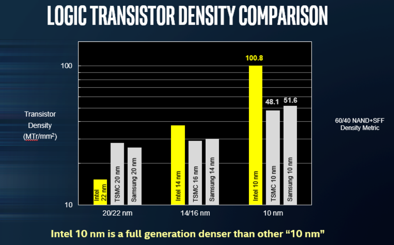
Why would they be worried? According to them, Intel’s 10 nm process utilizes third generation FinFET technology and is estimated to be a full
generation ahead of other “10 nm” technologies. The use of hyper scaling on Intel’s 10 nm technology extracts the full value of multi-patterning schemes and allows Intel to continue the benefits of Moore’s Law economics by delivering transistors that are smaller and have lower cost-per-transistor. Intel’s 10
nm process technology will be used to fabricate the full range of Intel products serving the client, server and other market segments.
The minimum gate pitch of Intel’s 10 nm process shrinks from 70 nm to 54 nm and the minimum metal
pitch shrinks from 52 nm to 36 nm. These smaller dimensions enable a logic transistor density of 100.8
mega transistors per mm2, which is 2.7x higher than Intel’s previous 14 nm technology and is
approximately 2x higher than other industry 10 nm technologies.
 
Intel referred to theirs as a 10-nm process, while GlobalFoundries called theirs a 7nm process. Who is right?
Intel-vs-GF-table-768x293.png
In other words, most parameters end up pretty darn close. (Comparison of the shrink from 14nm assumes they both mean the same thing with the 14nm designation.) Yes, there’s one outlier – metal 1 pitch – and yet, in that case, Intel’s 10nm process is more aggressive than GlobalFoundries’ 7nm version. So my question is why would Intel should be worried??????

Intel’s lead author, Chris Auth, said,

“I get this question a lot. Node names across the semiconductor industry have lost much of their meaning over the past 10 years.

“Intel has tried to follow historic trends and use node names that indicate ~0.7x linear scaling and ~0.5x area scaling for each generation (e.g. 22nm is 0.7x of 32nm). However, Intel’s recent 14nm and 10nm generations have each provided better than 0.4x area scaling due to aggressive scaling, so Intel node names are clearly conservative and don’t reflect the true area scaling benefit moving from node to node.”

GlobalFoundries had the following comment:

“We… feel that when comparing process nodes, it’s important to consider more than just transistor density. For instance, cost and complexity are two critical factors that are not considered in typical density metrics. Likewise, the timing of introduction is also important. The pure-play foundries have been accelerating their introduction of leading-edge nodes, while IDMs have been slowing down their cadence.
 
Just for general reference and something that is usually not really brought up: does anyone here REALLY know how to read those values and translate them to transistor/thermal performance or OC potential of a fully finished product?

At the end of the day, even if you provide numbers and comparisons to *all* of them in tables, can you even justify if a higher/lower number is better/worse for a particular workload, speed, load (as in voltage) or temperature?

The crux of the matter here is that, no matter how Intel wants to slice it, the processes are getting closer to each other. In fact, they're within striking distance and Intel has no distinctive advantage since no one knows how the marketed terms (FinFET v3, EUV, etc) will really perform until they start producing the silicon with those properties and produce something. Given Intel's own projections on the *performance* of the nodes, they'll be behind the 14nm process for a while when AMD has the design and just lacks the silicon to match Intel.

And all of that is not even counting that the CPU design itself must be aligned to the silicon properties!

Cheers!


logicdensity.png
Panic mode for what?...I hope you know that 7nm process does not actually mean """measured to be exactly 7 nanometers in diameter""" because nodes are not equal despite their similar ‘X nm’ marketing name being used by other companies to confuse and misguide customers. Process nodes used to represent the transistor gate length but this hasn’t been true since at least the late 1990s when some companies started to use different tactics while intel stayed closed to the actual numbers, on than graphic you can see the comparison between Intel's 10nm vs others 10nm(AKA 7NM) ..Fabs don’t follow a universal node naming process and a ‘10-nm’ grade transistor is significantly larger than 10 nanometers. How can you be so certain about GLOFLO 10nm (aka 7nm) reaching 5GHz? Same way people stated that Zen was a 5GHz processor then they said the same about Zen+ and here we are with only a few 250MHz increase still under 5GHz.
The 14 nm process being used by Intel has almost the same feature size compared to Samsung, Globalfoundries and TSMC’s 10nm nodes. Like others said, Intel’s 10nm was delayed but it will offer far superior transistor density (MTr/mm2) than any of their competitors 7nm


Y5BCDgHK5xGbl3a5.jpg
degFhsTxy31idMM2.jpg
3kWdPaLVolGDhCip.jpg
91dNBdhpyexYJDTE.jpg
8S7DWfQidto2DQQB_thm.jpg
 
Density has nothing to do with transistor performance, at all.

Intel has higher logic density than competing foundries, but lower SRAM density.

iedm-2017-intel-10-xtor-comparison.png


You can see the advantage Intel has in logic density, which is the more important metric here.

Transistor performance of 10nm+ nearly matches that of 14nm++, and it's over 2.5x as dense as 14nm++. 10nm++ will beat 14nm++ by a considerable margin in transistor performance.

No one in the industry has transistors that perform as good as 14nm++ yet, and that will be true until at least 2020 (when Intel releases their 10nm++ most likely).
 
Like Gon Freecss and others have pointed out intel has good advantage when it comes to density,And like I said before, The Problem here is that Intel's 14nm++ still offers more raw performance than current GLOFLO's 14mm and 12nm, Now they are not in a hurry just tweaking their 10nm.
 
Nothing of what you two posted really answers the points I raised as questions.

Having better density is good and all, but compared to what? FD-SOI at 32nm was better than Intel's 32nm with FinFET hands down, but it was a shame AMD had to use the BD uArch on top of it. IBM did take advantage of the good side of FD-SOI fully and produced really amazing CPUs with it for Mainframes.

So, again, do you know what TANGIBLE advantages all those numbers translate to? Projected density is fine, like I said, but there are OTHER properties that are as important as density. A single advantage doesn't mean they're ahead in overall performance for a node. Intel has already stated their 10nm node won't be better in all regards to 14nm++, so even if they're denser at 10nm, that won't translate into proper gains in certain markets. That is not what should make Intel shake, since it's projections, but the delays should. That means the WHOLE pipeline of products will get delays if they're not re-planned/re-purposed.

Cheers!
 
You just ignored the second part of my post.

10nm++ is projected to be better than 14nm++ all around (density, power, performance).

Jf71Tt4LHk44YR57.jpg


No one knows how other foundries' processes perform, but they're all gonna be weaker than 14nm++. Chances it'll take Intel's own 10nm++ process for the industry to break 14nm++'s transistor performance.
 

I see there is people that still believes all this Intel babbling. The problem (for Intel) is that TSMC and Samsung 10nm entered high volume production in 2016. Intel 10nm is not expected to enter high volume production until 2019 or 2020 (according to latest rumors) so, yes they are a generation ahead but, unfortunately, 3-4 years too late.
 
Intel Silently Launches Cannon Lake
David SchorMobile ProcessorsMay 15, 2018

As far back as Q4 2017, Intel mentioned that they have started shipping 10nm chips in low volume. Today, Intel has finally added the first 10nm chip to their database. Going under the same 8th Gen Core as Kaby Lake and Coffee Lake, the new Core i3-8121U which is based on the Cannon Lake microarchitecture has shown up on Intel’s ARK. Just don’t don’t get too excited because this thing is a major disappointment.
We have known about the Core i3-8121U SKU for quite some time now. In fact, we even added it to our site back in January but since it’s now on the official Intel website, we get to see the full specs; and it’s as bad as we all thought. For the most part, the specs are similar to Kaby Lake U models – 2 cores, 4 threads, and 15 W TDP. The L3 cache has been bumped to 4 MiB, matching current Coffee Lake U models (albeit those models are quad-core i3s). This processor comes with the chipset in the same BGA package and features 16x PCIe lanes, which is 4 more lanes than Kaby Lake U models but comparable to current Coffee Lake U models. Interestingly, this model has a junction temperature of 105 degrees (C) versus 100 on current Coffee Lake U models. One of the main features that were added to Cannon Lake is the new support for LPDDR4/LPDDR4X memory with rates up to 2400 MT/s.

There are a number of odd details about this model. For a few months now, it has been rumored that Intel qualified a dual-core model with a non-working GPU. What’s interesting is that there is no integrated graphics listed in ARK either. Additionally, there is also no mention of AVX-512 support which was supposed to be introduced with Cannon Lake for client models according to Intel’s official ISA documents.
https://fuse.wikichip.org/news/1285/intel-launches-cannon-lake/
 
Copy and pasting Intel PR statements does not change the fact that the 10nm part released is being called "a turd" in social media! When was 10nm supposed to launch, 2016? I have some swamp land in Florida I want to sell you guys! It's prime real estate! I have graphs and charts to prove it trust me I wouldn't lie to you! It's been ready for sale since 2016!
 

There is no "diameter" in transistors, in the past it used to be gate lenght but it's not anymore (not even for intel). And yes, we know intel's 10nm are not really 10nm while TSMC 7nm are not really 7nm, but foundries 7nm ofer similar density to intel 10nm, with the diferences that at least TSMC 7nm entered high volume production last month, while intel similar 10nm will not enter high volume production at least in a year or year and a half.

You are makeing a terrible mistake here, this graphs is comparing what intel's call 10 nm with what TSMC/Samsung call 10nm. TSMC 7nm is way denser than that at aproximately 100 Mtr/mm2. Again with the problñem that TSMC already entered high volume production while intel has to wait 1 year or more.

I'm not certain of that, that is why i wrote RUMOR. I expect people can notice the diference between FACT and RUMOR. By the way I expected 4.4 to 4.5 GHz for zen+. I was optimistic, but got very close.

Wrong, intels 10 nm will ofere similar transistor density to foundries 7nm but will start high volume production 1 to 2 years later.


And your base for all these are called rumors? Okay got it..


Oh yes social media, remind me again how much I love social media..


I guess that asking you to look at the previous graphs that shows Intel's 10nm density advantage over GLOFLO 7nm provided by me and Gon Freecss is to much to ask right?..


No, I didn't. I'm talking about 10nm vs 14nm++, since 10nm++ is not even being worked on at the moment; a projection is hardly accurate enough to say it will be a "winner node". Has Intel even mentioned anything beyond 10nm with a potential time-to-market anyway? We have time-less projections, but nothing else. And if you quote 2017 roadmaps, then 10nm should already be in HVM, but it is not.

So, you guys can put as many numbers around the process as you want and keep saying "everything is fine", but when reality catches up to Intel (which, it seems it already has, since they're shuffling people around) you'll see changes in the roadmaps. That should be happening very soon.

Cheers!


Just to clarify:
Intel current 10nm yield is rumored to be in the single digits, and volume production is rumored to be delayed till 2020. Intel just released a 10nm i3 that has worse specs than Kaby Lake with a disabled iGPU seems to fit those rumors of bad yields. BK in a recent earning calls said he didn't know when 10nm volume production will start. He said it could be first or second half of 2019 depending on yields. If yields are as rumors suggest, single digit, then the rumor of 2020 volume production looks good as well.
 
Status
Not open for further replies.