


Well, reading a book does not always clarify concepts and sometimes it might be confusing when the author deep dives into the technical concepts. I hope some of the knowledgeable techs or gurus could shed some lights on the concepts and the questions I ask.
- Where is the multiplier located? Is it located inside the CPU or the CPU package? Or is it on the motherboard? But if it is inside the CPU, how come people always say things such as changing the multiplier of the motherboard? This is the first confusing concept.
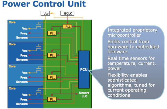
- Baseclock. Is baseclock (BCLK) only related to the CPU or the whole system? How come people say well if you wanna overclock, you could do so with the baseclock?
- According to the book, the author states (Michael Meyer) that, when he talks about RAM, "When the CPU needs certain bytes of data, it requests those bytes via the address bus. The CPU does not know the physical location of the RAM that stores that data, not the physical makeup of the RAM - such as how many DRAM chips work together to provide the 64-bit wide memory rows. The Memory controller chip keeps track of this and just gives the CPU whichever bytes it requests." The question is if the CPU does not know the address, how can it request the data? Likewise, how can it also send data to the memory?


 Twitter